
Full datasheet walkthrough — Dk, Df, CTE, thermal conductivity — plus the production guidelines that make RO4350B builds reliable.
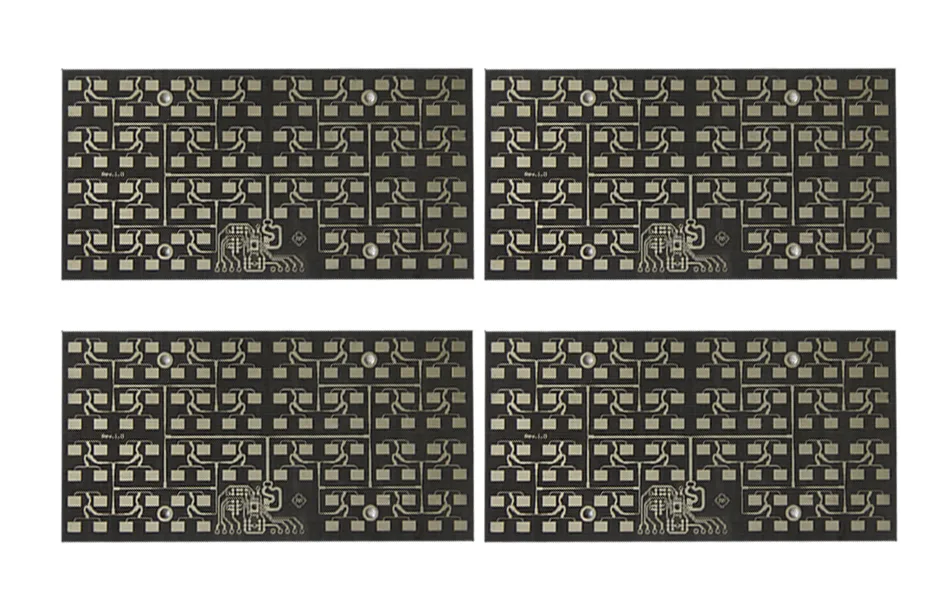
Bottom line up front: RO4350B is a high-frequency laminate that combines premium RF performance with standard FR4 process compatibility — Dk 3.48 ± 0.05, Df 0.0037, CTE matched to copper, and UL 94 V-0 compliance. It spans wireless infrastructure, automotive radar, 5G, high-performance computing, and defense electronics. The production keys: impedance-first design, controlled drilling, low-temperature lamination below 288°C, and network-analyzer verification.
This article details the parameters, application fields, and production guidelines.
The numbers that define the material:
| Parameter | Value | Design benefit |
|---|---|---|
| Dielectric constant (Dk) | 3.48 ± 0.05 @ 10 GHz | Precise impedance control in RF circuits |
| Dissipation factor (Df) | 0.0037 @ 10 GHz | Minimal signal loss at high frequency |
| CTE (X/Y) | 11 ppm/°C | Closely matches copper for thermal stability |
| CTE (Z) | 32 ppm/°C | Improved multilayer reliability |
| Thermal conductivity | 0.62 W/m·K | Moderate thermal management support |
| Water absorption | 0.06% | Dimensional and electrical stability in humidity |
| Copper foil range | 0.5 oz – 2 oz | Flexibility across design needs |
| Flammability | UL 94 V-0 | High safety compliance |
Processing characteristics complete the picture: mechanical drilling and laser cutting are both supported, and the wide copper foil range (0.5–2 oz) covers diverse design needs.
Design phase: impedance matching is crucial — model with professional electromagnetic simulation tools (HFSS or ADS). Hybrid stackups with FR4 balance cost and performance, but CTE differences must be addressed to avoid warping or delamination.
Material cutting: laser or precision mechanical cutting keeps edges smooth on this flexible material; deburr immediately to maintain dimensional accuracy.
Drilling and PTH: reduce drill speed to minimize heat impact on the material; ensure smooth hole walls for optimal conductivity and plating strength.
Lamination and bonding: use low-temperature lamination below 288°C to prevent delamination or performance degradation, with uniform heating and appropriate pressure for strong bonding.
Surface treatment: ENIG, immersion tin, and OSP are standard — avoid high-temperature chemical solutions that could deform the material.
Testing and QC: finished boards are evaluated on a high-frequency network analyzer for dielectric constant, loss factor, and impedance consistency, plus thermal cycling tests for high-temperature and mechanical stability. We hold impedance to ±10% with coupon verification.
XCE PCB manufactures RO4350B boards from 2 to 72 layers, panels up to 600×1200 mm, with prototypes in as fast as 24 hours to IPC-A-600G criteria.
RO4350B’s recipe is proven: tightly specified electricals, copper-matched CTE, and FR4-compatible processing that keeps cost down. Follow the production guidelines — simulation-backed impedance design, controlled drilling, low-temperature lamination, network-analyzer QC — and the material delivers reliably across communication, automotive, 5G, computing, and defense applications. Send us your stackup for a manufacturability review and quote.
Send us your Gerber files and requirements for a manufacturability review and a tailored quotation.