
Most capability tables are a wall of numbers with no tolerances, no test method and no definition of what ‘general’ means. This page reads our own capability table the way an experienced buyer should read any supplier’s: row by row, with the physics and the audit questions behind each number. XCE PCB has manufactured high-frequency PCBs since 2009 on a 5,000 m² floor with 80+ engineers and a monthly output of 10,000 m².
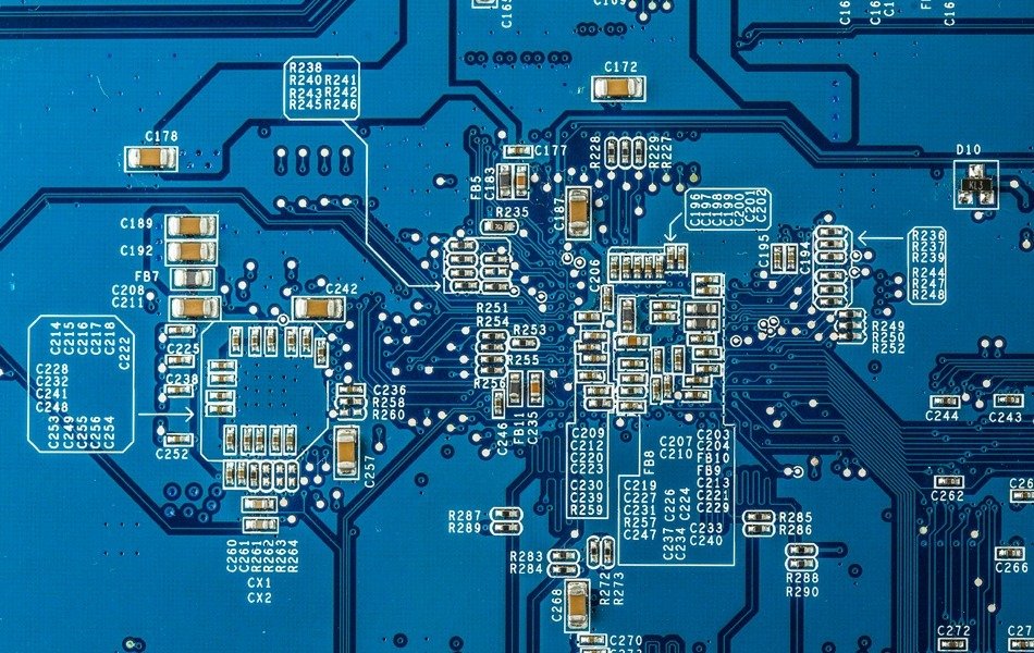
XCE PCB Processing Capability at a Glance
Here is the table, stated with the two things most tables leave out: what is measured and what the number covers. Every row below is expanded in the sections that follow.
| Item | Capability | Notes |
| Layer count | 2 – 72 layers | RF, hybrid, microwave and multilayer HDI |
| Maximum panel size | 600 x 1200 mm | Usable area is smaller; see panel section |
| Impedance control | ±10% | TDR coupon per batch on request |
| Minimum drilled hole | 0.2 mm standard, 0.1 mm capable | PTFE aspect ratio kept ≤ 6:1 |
| Finished board thickness | 0.1 – 12 mm | Extreme thicknesses need a stackup review |
| Copper weight | 0.5 – 5 oz | Base 1 oz = 35 µm; see current table |
| Sample turnaround | As fast as 24 h | Stocked material, simple stackup |
| Material stock | Rogers / Taconic / F4B / TP-2 / FR-4 | Dk 2.2 – 10.6 in regular stock |
| Acceptance standards | IPC-A-600G, IPC-6015 | Class 2 standard, Class 3 on request |
| Scale | 5,000 m² facility, 10,000 m²/month | 80+ engineers, operating since 2009 |
If you just want the raw list, see our process capability page. The rest of this article is the version with the fine print, because that is where quotes go wrong.
Layer Count: What 2-72 Layers Really Means
A 72-layer claim is only meaningful if the shop can name the constraint that limits it. For RF work that constraint is rarely the press; it is the interaction between layer count and material. Every additional sub-lamination adds a thermal cycle, and PTFE-based laminates only tolerate a limited number of reflows before plated-hole reliability suffers. High Z-axis expansion materials expand far more than FR-4 across a reflow peak, which is why we cap PTFE aspect ratios at 6:1 and review any high-layer-count PTFE stackup before committing.
The practical guidance: 2 to 20 layers of RF/hybrid construction is routine work. Above 40 layers, expect the conversation to shift from price to stackup engineering – registration tolerances, buried via fill and lamination sequence. A supplier who quotes a 60-layer hybrid board in one email without asking for the stackup is quoting a guess.
Panel Size: 600 x 1200 mm Is Not Usable Board Area
Our maximum panel is 600 x 1200 mm, but the usable area per job is smaller by the tooling rail, coupon zones and breakaway edges. Two more effects quietly eat margin on large RF panels. First, prepreg shrinkage of 0.02 – 0.05% moves a 600 mm span by 0.12 – 0.30 mm, which matters when inner-layer artwork must stay registered to a PTFE core. Second, laminates expand thermally: a 600 mm span of a low-Dk PTFE material moves roughly 0.3 mm across a 20 °C swing, so we hold large-panel tolerances at a defined temperature, not ‘room temperature’.
When you size a design near the panel limit, tell the supplier early. The answer changes the panelization plan, the coupon placement and sometimes the layer count.
Impedance Control: What ±10% Actually Covers
We hold controlled impedance to ±10% of your target. That number is only honest if you know what feeds it. Laminate thickness tolerance is usually the largest term: a ±10% dielectric thickness variation moves impedance by roughly ±6% on a typical microstrip. Etch compensation comes next – a ±25 µm trace-width variation shifts a 0.254 mm line by about ±2.8%. Solder mask over the trace typically pulls impedance down 1 to 3 ohms, which is why bare coupons read slightly high versus finished boards. A missed bond-ply layer in the stackup file can add 20% on its own.
This is why we verify with a TDR coupon from the same panel rather than calculating alone. For a deeper treatment of the design side, see our article on high-frequency PCB impedance control.
Material Stock: Dk 2.2-10.6 and What It Means for Lead Time
Regular stock across Rogers, Taconic, F4B, TP-2 and FR-4 covers dielectric constants from 2.2 to 10.6. The range is not random – it maps the standard RF material ladder:
| Material | Dk | Position |
| RT/duroid 5880 / TLY-5 / F4BM220 | 2.20 | Lowest-loss PTFE class, antennas and long runs |
| RO3003-class ceramic-filled PTFE | 3.00 | Tight Dk tolerance for phase-critical designs |
| RO4350B-class hydrocarbon | 3.48 | FR-4-like processing, mid-loss |
| RO3010 / 6010-class | 10.2 | Miniaturization where Df is secondary |
Stock matters twice: it enables 24-hour sampling, and it means the material datasheet we design against is the one we actually process. For the processing differences, read our guides on RT/duroid 5880, Taconic laminates and RO4350B production. Mixing PTFE with FR-4 in one stackup is its own discipline – see the F4B hybrid lamination guide.
Copper Weight and Current Capacity
We process 0.5 to 5 oz finished copper. Three numbers matter when you design power or current-carrying RF structures:
| Item | Value | Note |
| Base copper (1 oz) | 35 µm | Outer layers plate to 50 – 60 µm after patterning |
| Current at 10 °C rise, external 1 oz | ~2.3 A | 2 oz ~4.0 A, 6 oz ~8.8 A (IPC-2221 chart) |
| Internal layers | ~half of external | Reduced heat dissipation; plan early |
Heavy copper also changes etch: with 2 oz copper, sidewall etch of about 28 µm per side sets a practical floor on fine lines. If your design pairs 0.15 mm traces with 2 oz copper, expect that conversation during DFM.
Surface Finishes: Match the Finish to the Loss Budget
We offer ENIG, gold plating, immersion silver, silver plating, HASL, gold finger, OSP, nickel-palladium gold, resin plugging and combinations such as ENIG plus hard gold. For RF boards the finish is an electrical decision, not a cosmetic one:
| Finish | Best for | Watch-out at RF |
| OSP | Lowest added loss | Limited reflow cycles, no wire bonding |
| Immersion silver | Low loss plus solderability | Requires sulfur-free packaging |
| ENIG | Flatness, fine pitch, shelf life | Nickel skin adds conductor loss above 10 GHz |
| HASL | Cost, prototyping | Uneven surface, poor for controlled impedance |
At 10 GHz the skin depth in copper is about 0.65 µm and in nickel about 1.33 µm, so ENIG pushes signal current into the nickel layer and raises conductor loss. For millimeter-wave work we usually recommend OSP or immersion silver. The full comparison is in our article on surface treatment processes.
Sampling in 24 Hours: What It Covers
As-fast-as-24-hour sampling applies to designs on stocked laminate with a stackup we can run on our standard flow. It is a real commitment, not a teaser – our 5,000 m² facility runs the full sequence in-house from imaging to e-test, which is what makes one-day turnaround possible at all. What it does not cover: customer-ordered laminate, hybrid stackups needing sequential cure, and coupon TDR reporting on top of a same-day ship. We would rather give you a realistic date in the quote than a heroic date in the email.
If you are new to RF sourcing, our overview of what makes a PCB an RF board explains why these process steps differ from standard FR-4 work, and our article on high-frequency PCB characteristics covers the material side.
A 12-Point Supplier Audit Checklist for RF PCB Buyers
Use this list on any RF PCB supplier, including us. A capable shop answers every row with a document or a measurement, not an adjective.
| # | Ask | A good answer looks like |
| 1 | Layer range claim | A reference board above 40 layers with photos or report |
| 2 | Impedance tolerance | ±10% stated with TDR coupon reports per batch |
| 3 | Panel vs usable area | Tooling margin and coupon zones disclosed |
| 4 | Material inventory | Named laminates in stock, not ‘we can order’ |
| 5 | PTFE hole preparation | Sodium naphthalene or plasma desmear on the line |
| 6 | Aspect ratio limits | ≤ 6:1 for PTFE stated as an engineering rule |
| 7 | Hybrid lamination | Separate cure windows for FR-4 / RO4000 / PTFE systems |
| 8 | Low-loss finishes | OSP and immersion silver offered alongside ENIG |
| 9 | Acceptance standards | IPC-A-600G / IPC-6015 inspection criteria named |
| 10 | Quick-turn terms | 24 h sampling defined: which designs qualify |
| 11 | Engineering support | Stackup review and DFM feedback before the PO |
| 12 | Scale evidence | Facility size, monthly output, engineer count, years operating |
How to Send a Drawing for a Fast, Accurate Quote
Five items let us quote in one pass instead of three emails: Gerber or ODB++ data, the stackup with material callouts, your impedance table, copper weights per layer, and quantity plus target delivery. If the impedance table is missing, say which nets are controlled – we will propose targets and confirm them before release, which is faster than discovering the miss after etch. Send them through our quote form and an engineer, not a sales script, will review the stackup.
For broader context on material selection, our articles on Rogers and Taconic laminates show how we read datasheets against real process windows – the same discipline we apply to every incoming drawing.
Frequently Asked Questions
What is your maximum layer count for RF boards?
How fast can you deliver samples?
What impedance tolerance do you guarantee, and how is it verified?
Can you build hybrid stackups, such as PTFE bonded to FR-4?
Which laminate brands do you keep in stock?
What files do you need for an accurate quote?
Need a 2-72 Layer RF Board Quoted?
Send us your Gerber files and requirements for a manufacturability review and a tailored quotation.
sales1@xcepcb.com
+86 180 3341 4657