
Discover what truly matters in high frequency PCB manufacturing. Learn how ±3% impedance control, ±1mil trace accuracy, VNA testing, Rogers PCB materials, and RF PCB expertise impact microwave, 5G, antenna, and power amplifier performance.
HighFrequency PCB Manufacturing: Why ±3% Impedance Control and VNA Testing Matter More Than Lead Time
For RF, microwave, and antenna engineers, choosing a high frequency PCB manufacturer should never start with one question:
“How fast can you deliver?”
The real question is:
Can the PCB actually perform at 5.8GHz, 24GHz, 60GHz, 77GHz, or even higher frequencies?
Because in RF engineering, a board that merely passes continuity testing is not necessarily a board that performs correctly.
After years of manufacturing microwave PCBs, RF power amplifier boards, antenna arrays, and multilayer Rogers hybrid structures, we have learned that engineers care far more about impedance consistency, insertion loss, and measurement data than marketing claims.
Let’s talk about the specifications that actually determine whether a high frequency PCB works in the real world.
Why Impedance Control Matters More Than Most People Think
Many PCB suppliers advertise impedance control capabilities.
However, there is a significant difference between controlling impedance within ±10% and controlling it within ±3%.
For RF systems such as:
Power amplifiers
Power dividers
Directional couplers
Phase shifters
4G antenna systems
5G antenna arrays
small impedance variations can directly impact:
Return loss
VSWR
Phase consistency
Radiation efficiency
Power transfer efficiency
A transmission line designed as 50Ω should behave as closely as possible to 50Ω throughout the entire signal path.
At XCEP PCB, typical controlled impedance requirements include:
Standard RF applications: ±5%
Advanced microwave applications: ±3%
This tighter control helps maintain signal integrity across multiple RF channels and improves phase matching performance in antenna and beamforming systems.
For more information about controlled impedance PCB fabrication, visit:
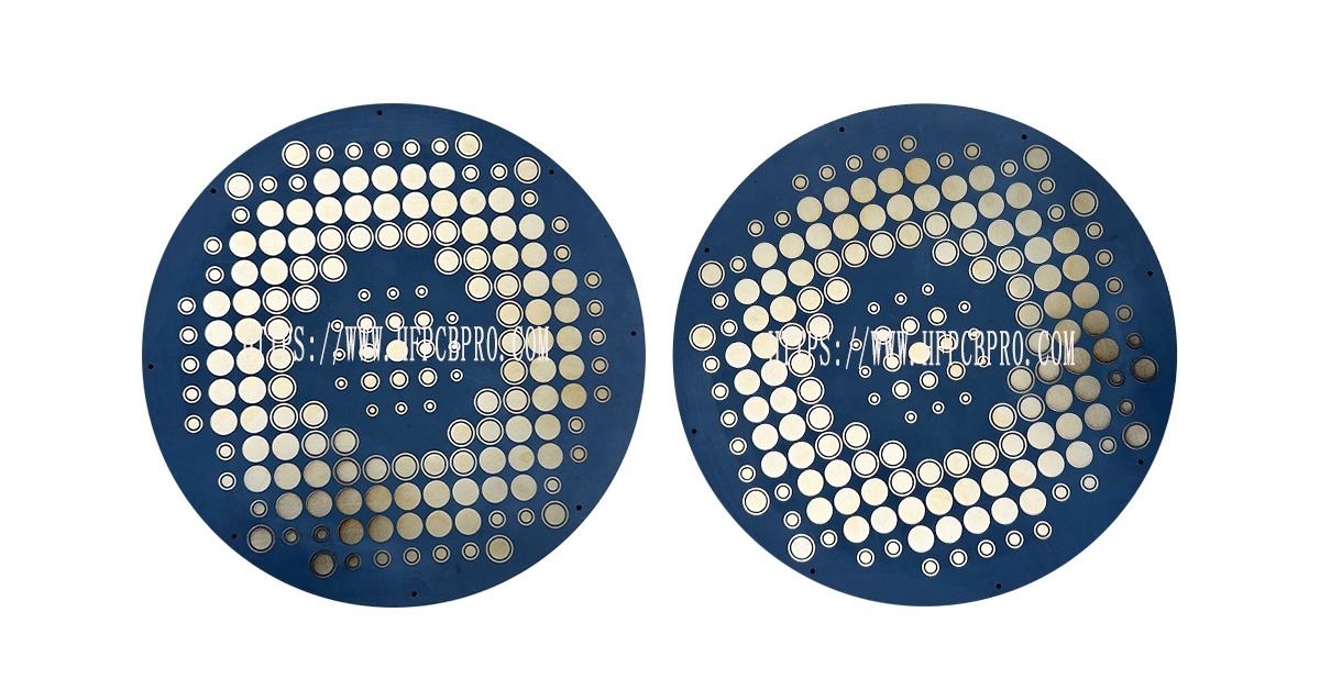 Controlled impedance test coupon used for RF and microwave PCB manufacturing.
Trace Width Accuracy Directly Affects RF Performance
One of the most overlooked factors in RF PCB manufacturing is trace geometry.
A designer may calculate a 50Ω microstrip line with precise dimensions, but if the final etched conductor deviates significantly from the intended width, the impedance changes accordingly.
Poor etching processes often produce:
Excessive undercutting
Trapezoidal conductor profiles
Inconsistent conductor widths
Increased insertion loss
For high frequency PCB applications, we maintain trace width tolerances as tight as:
±1mil (±0.025mm)
This level of precision is particularly important for:
Microstrip antenna arrays
RF power amplifier boards
Microwave filters
High-frequency matching networks
Rogers multilayer hybrid boards
PTFE-based RF structures
When internal layer trace widths drift outside tolerance, overall RF performance can deteriorate quickly.
This is why advanced RF PCB manufacturing requires both process control and material expertise.
Flying Probe Testing Is Only the Beginning
Many manufacturers claim they perform electrical testing.
In reality, most testing only verifies:
Open circuits
Short circuits
Net connectivity
While important, these tests do not tell engineers whether the RF board will perform properly at operating frequencies.
A high frequency PCB can pass every continuity test and still fail in real-world RF applications.
The parameters that truly matter include:
Insertion loss
Return loss
VSWR
Phase consistency
Dielectric loss performance
This is where Vector Network Analyzer (VNA) testing becomes essential.
 Vector Network Analyzer testing insertion loss and return loss on an RF PCB sample.
Why VNA Testing Reveals the Real Performance of a High Frequency PCB
Unlike conventional electrical testing, a Vector Network Analyzer measures actual RF behavior.
Engineers can evaluate:
S11 (Return Loss)
S21 (Insertion Loss)
VSWR
Phase response
Frequency-dependent performance
Questions that can only be answered through VNA testing include:
Is the dielectric loss higher than expected?
Is the antenna feed network performing correctly?
Does the power divider meet insertion loss specifications?
Are microwave transmission paths behaving as designed?
For critical projects, measured data often provides more value than manufacturing specifications alone.
Depending on project requirements, test reports can include:
Material identification
Insertion loss measurements
Return loss measurements
Frequency response data
RF performance validation
This allows engineering teams to make decisions based on measured performance rather than assumptions.
For PCB manufacturing process details, visit:
Why Hybrid RF Stackups Are More Difficult Than Standard RF Boards
Many PCB manufacturers can fabricate simple two-layer Rogers boards.
The real challenge begins when multiple materials must coexist in one stackup.
Examples include:
Rogers + FR-4 hybrid constructions
F4BM hybrid multilayer boards
Thick copper RF power boards
RF and digital mixed-signal platforms
Each material has unique characteristics:
Thermal expansion coefficients
Resin flow properties
Lamination behavior
Mechanical stress responses
Improper process control may result in:
Delamination
Warpage
Registration shifts
Impedance variation
Over the years, we have successfully manufactured numerous:
Rogers hybrid multilayer PCBs
Thick copper RF boards
PTFE multilayer structures
Microwave power amplifier PCBs
Base station antenna boards
The key lies in understanding how different materials behave during lamination and compensating accordingly.
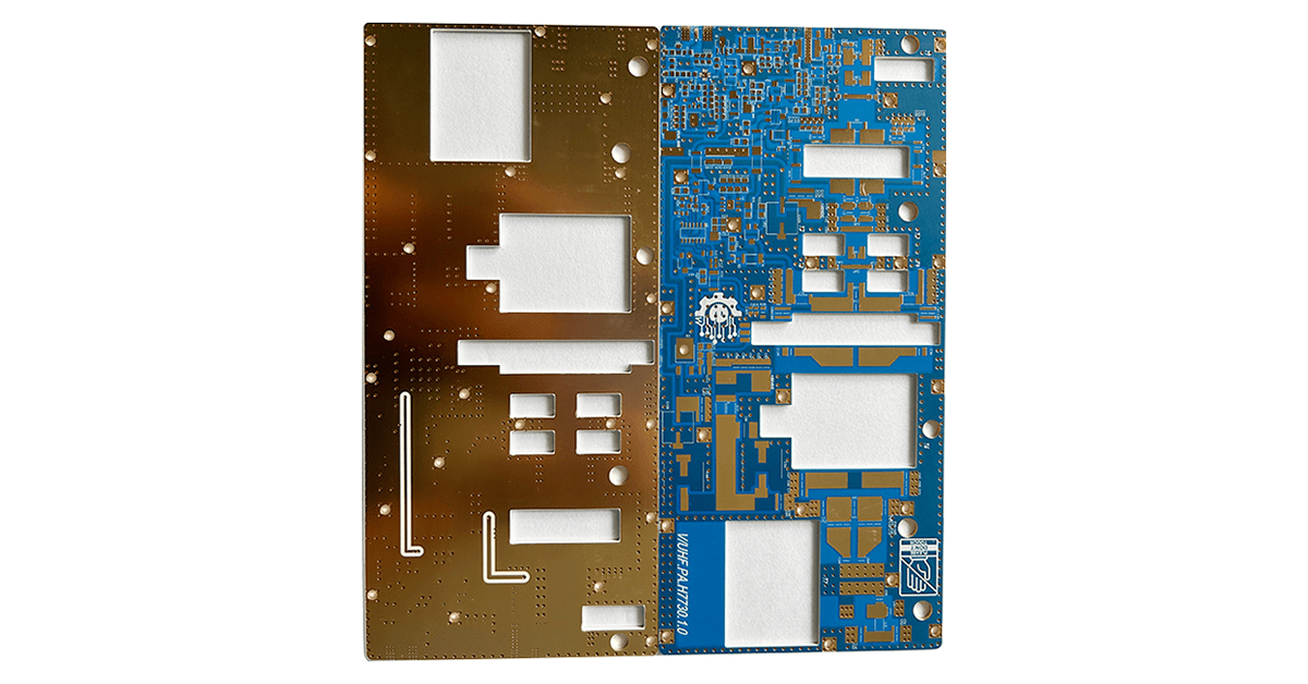 Rogers and FR-4 hybrid multilayer PCB structure used in advanced RF communication systems.
Common High Frequency PCB Materials We Work With
Depending on frequency requirements and budget considerations, common material options include:
Rogers Series
RO4003C
RO4350B
RO5880
RO6002
RO6010
Learn more:
https://szxcepcb.com/processing-capability/
Taconic Materials
RF-35
TLX Series
TLC Series
Arlon RF Materials
CLTE Series
AD Series
Domestic RF Alternatives
F4B
F4BM
ZYF Series
These materials are widely used in:
RF power amplifier boards
Microwave communication systems
Satellite communication equipment
Radar systems
4G and 5G antennas
Military RF electronics
Engineering Results Matter More Than Marketing Claims
Engineers are rarely impressed by factory size.
What they want is straightforward:
Accurate impedance
Stable RF performance
Tight trace width control
Reliable manufacturing consistency
Measured test data
When a PCB arrives with verified impedance performance and documented RF measurements, engineering validation becomes significantly easier.
Ultimately, successful RF projects are built on repeatable manufacturing quality, not promises.
If your next project involves a 5G antenna, microwave amplifier, beamforming array, coupler, or radar system, the most important question may not be lead time.
It may be whether the PCB can actually deliver the performance your design requires.