
Eight manufacturing precautions and six application areas — how four-layer double-sided RF boards are built and where they earn their keep.
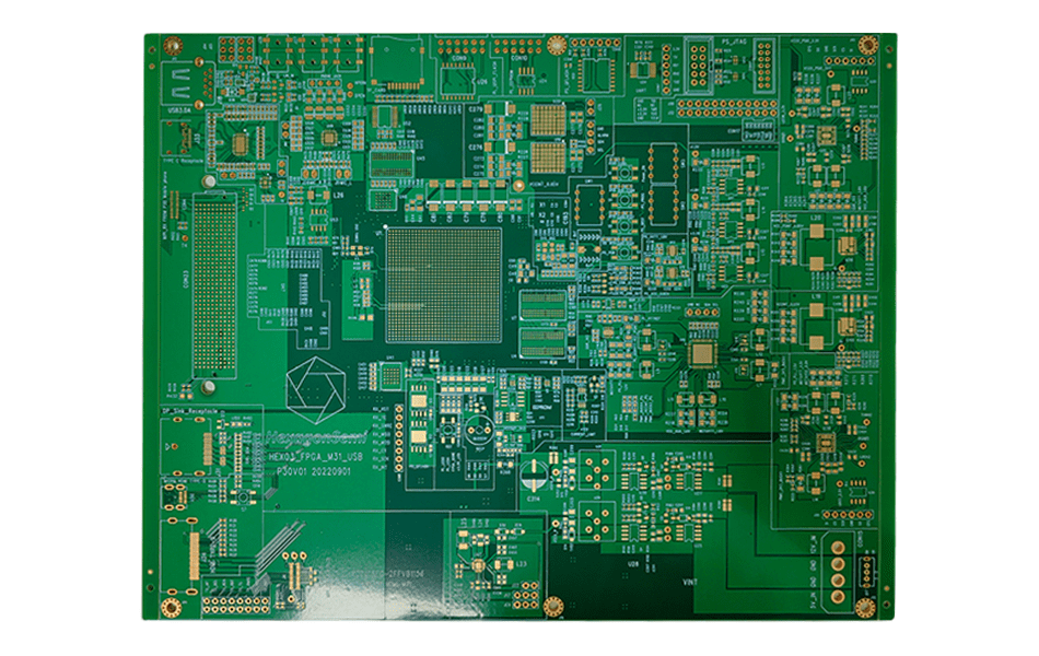
Four-Layer Double-Sided High-Frequency PCBs: The Short Answer
Bottom line up front: a four-layer double-sided high-frequency PCB earns its keep where standard FR-4 boards cannot — high-frequency signal transmission with high reliability. The classic stack-up puts signal layers inner, ground and power outer for shielding; manufacturing demands strict material, lamination, drilling, and impedance control. Applications concentrate in wireless communication, radar and navigation, satellite links, medical imaging, automotive electronics, and industrial automation.
This article walks through the eight processing precautions and six application areas in detail.
Precaution 1–2: Material Selection and Stack-Up Design
Materials: common choices include PTFE, ceramic-filled PTFE, and fluororesin — low-loss materials whose Dk and Df directly impact signal transmission. Look for low loss, high stability, and high-temperature resistance, and make sure CTE values match across the stack to avoid temperature-driven delamination.
Stack-up: the four-layer structure typically separates signal, ground, and power layers to reduce crosstalk and reflection. Signal layers go inner, with ground and power outer for shielding and stable current paths; layer spacing and copper foil thickness are optimized against impedance specifications.
Precaution 3–4: Lamination and Drilling
Lamination: temperature and pressure must be strictly controlled — too hot decomposes the material, too cool bonds weakly. Gradual and vacuum lamination reduce bubbles and delamination, with CTE differences between materials considered to prevent interlayer separation.
Drilling: through-, blind, and buried vias all appear in four-layer builds. High-frequency materials are typically hard, causing burrs and rough hole walls; precision drill bits and parameter control reduce defects, and laser drilling achieves smoother hole walls that effectively reduce signal loss.
Precaution 5–6: Impedance Control and Surface Treatment
Impedance control: line width, spacing, interlayer distance, and dielectric are precisely calculated, usually with simulation tools, then verified by impedance testing during production — we hold ±10% with a measured coupon on every panel.
Surface treatment: finishes must add low signal loss and good oxidation resistance. Options include chemical gold (ENIG), chemical silver, tin, and nickel-gold plating — chemical gold is the preferred choice for high-frequency boards, reducing contact resistance with excellent conductivity for long-term operation.
Precaution 7–8: Testing, ESD and Quality Control
Signal integrity testing: reflection coefficient, transmission loss, crosstalk, and delay are evaluated — S-parameter testing with specialized equipment confirms performance under high-frequency conditions.
ESD and EMI prevention: anti-static wristbands and mats prevent static buildup during handling; well-designed grounding layers and shielding materials reduce electromagnetic interference.
Quality inspection: AOI, electrical testing, X-ray, and interlayer alignment inspection verify the finished board — X-ray confirming blind/buried via alignment accuracy.
Application Areas
Six fields dominate demand for these boards:
| Application area | Typical equipment | What the board provides |
|---|---|---|
| Wireless communication | Base stations, 5G antennas, Wi-Fi routers | Reduces attenuation for stable transmission at high frequencies |
| Radar & navigation | Radar antennas, navigation receivers | Signal clarity and positioning accuracy |
| Satellite communication | Receivers, antennas, core modules | Low loss and anti-interference in extreme conditions |
| Medical equipment | CT, MRI imaging systems | Stable transmission for clear, precise imaging |
| Automotive electronics | Car radar, navigation, communication modules | Reliable high-speed transmission for smart vehicles |
| Industrial automation | High-frequency measurement, wireless data links | Data speed and stability for industrial control |
The pattern: anywhere high-frequency signals meet interference, four-layer double-sided high-frequency boards reduce attenuation and stabilize transmission.
How XCE PCB Builds Them
XCE PCB manufactures high-frequency boards from 2 to 72 layers, panels up to 600×1200 mm, with prototypes in as fast as 24 hours to IPC-A-600G criteria — four-layer double-sided builds are a core product, with ENIG finish and coupon-verified impedance as standard.
Conclusion
Four-layer double-sided high-frequency PCBs succeed on eight disciplines — material, stack-up, lamination, drilling, impedance, surface finish, testing, and ESD/EMI control — and serve six demanding fields from 5G base stations to MRI machines. If your product needs this class of board, send us your stackup; our engineers will review manufacturability and quote with the process plan attached.
Frequently Asked Questions
Why put signal layers inner in a four-layer high-frequency PCB?
What surface finish is best for four-layer high-frequency PCBs?
Why is laser drilling used on high-frequency materials?
How is signal integrity verified before shipment?
How fast can you build four-layer high-frequency prototypes?
Need Four-Layer High-Frequency Boards?
Send us your Gerber files and requirements for a manufacturability review and a tailored quotation.
sales1@xcepcb.com
+86 180 3818 8537