
From FR-4 country roads to F1 racetracks — what high-frequency PCBs are, where 5G and AI are taking them, and the three challenges still being solved.
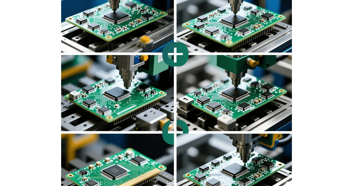
The Unsung Hero of the 5G and AI Era
Inside smartphones, Wi-Fi networks, 5G base stations, autonomous vehicles, and AI systems, vast amounts of data travel invisibly at incredible speeds as high-frequency electromagnetic waves. Carrying and guiding these high-speed convoys is a special class of circuit board: the High-Frequency PCB — the indispensable, unsung hero of the connected age. This article explains what makes these boards special, where the technology is heading, and the challenges that remain.
Why a Standard FR-4 Board Falls Short at GHz
Imagine a standard FR-4 circuit board as a bumpy, gravel-filled country road, while a high-frequency PCB is a smooth, solid, low-friction F1 racetrack. When signal “vehicles” are slow (low frequency), the country road works. But at GHz frequencies, three problems become glaring:
| Problem (FR-4) | How it shows up | The high-frequency answer |
|---|---|---|
| Signal loss | “Soft” substrate absorbs signal energy as heat | Ultra-low Df lets signals pass with minimal resistance |
| Signal distortion | Uneven “road surface” bounces waveforms, phase chaos | Stable dielectric keeps signals synchronous and in phase |
| Impedance control | Dielectric properties drift with frequency and temperature | Highly uniform structure enables precise, matched transmission lines |
The answer lies in specialized laminates — the renowned Rogers and Taconic families — whose three advantages define the category: ultra-low dissipation factor (energy goes to transmission, not heat, preserving range and signal quality), stable dielectric constant (a never-shrinking ruler for precise design, signals arriving synchronously and in phase), and excellent impedance control (uniform board structure lets manufacturers build transmission lines with extreme precision — signals navigate turns without reflecting).
Trend 1–3: Where the Technology Is Heading
With 5G, IoT, AI, and autonomous driving exploding, high-frequency PCBs are in a golden age marked by three trends:
| Trend | What it means |
|---|---|
| Material innovation | New composites and ceramic-filled materials with steadier Dk and lower loss for 6G and terahertz imaging |
| Integration with ICs | System-in-Package and Antenna-in-Package: chips, antennas, and passives integrated on the board — ideal for smartphones and micro-base stations |
| Higher frequency, more power | mmWave radar and 5G base stations above 24 GHz demand stable performance plus thermal management headroom |
The integration trend is the most visible: the board evolves from a passive carrier into a functional miniature system — which is exactly why fabricator capability now reaches into assembly-level questions, not just etching.
Challenge 1: The Cost Dilemma
High performance comes at a high price. Raw materials — specialty polymers, precision ceramics — are costly, and the manufacturing processes demand advanced equipment and highly skilled technicians, pushing finished prices far above standard PCBs. Finding the balance between high performance and low cost is the key to mass adoption; hybrid stackups (an RF layer over FR-4 cores) are the pragmatic answer for multilayer builds.
Challenge 2: The Precision Manufacturing Hurdle
High-frequency circuits demand micrometer-level machining accuracy. Any minor variation in trace width, inconsistency in dielectric layer thickness, or increased surface roughness causes a sharp performance decline. Every process step — drilling, patterning, lamination, surface finishing — is challenged. This is why we hold impedance to ±10% with a measured coupon on every panel, and verify rather than assume.
Challenge 3: Reliability and Integration
In the multi-physics environment of high frequency, high speed, and high power, three questions never close: how to ensure material long-term stability; how to resolve internal stresses from mismatched coefficients of thermal expansion between different materials; and how to manage the more complex heat dissipation that integration brings. These are the problems engineers work on daily, in labs and on production lines — environmental testing and CTE-matched stackup design are the current state of the art.
What This Means for Your Design
The practical takeaways: pick the material for the frequency band, not the brand; plan thermal management together with the stackup; and involve your fabricator before the design freezes — cost and manufacturability are decided at stackup time.
XCE PCB manufactures high-frequency boards from 2 to 72 layers, panels up to 600×1200 mm, with impedance held to ±10% and prototypes in as fast as 24 hours to IPC-A-600G criteria.
Conclusion
Hidden inside devices, high-frequency PCBs form the backbone of modern wireless communication and high-speed computing — from the phone in your hand to the autonomous vehicles of the future. Cost, precision, and reliability challenges are real, but materials science and manufacturing advances keep widening this information superhighway. If your product rides that highway, send us your stackup; our engineers will review it and quote with the process plan attached.
Frequently Asked Questions
Why can't standard FR-4 handle high-frequency signals?
What makes high-frequency PCB materials special?
How will high-frequency PCBs evolve with 6G and AI?
Why are high-frequency PCBs expensive?
How fast can you prototype high-frequency boards?
Building for the 5G and AI Era?
Send us your Gerber files and requirements for a manufacturability review and a tailored quotation.
sales1@xcepcb.com
+86 180 3341 4657