
Through, blind, buried, and microvias — the four hole types that define RF board interconnects, their functions, and how each is manufactured.
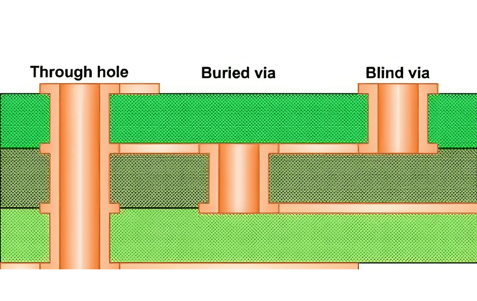
Hole Types in High-Frequency PCBs: The Short Answer
Bottom line up front: four hole types cover high-frequency PCB interconnects — through holes, blind holes, buried holes, and microvias. Each has a distinct geometry, function set, and manufacturing process: through holes for layer-to-layer connectivity and heat, blind and buried holes for space-saving density, microvias for HDI performance. Choosing among them is a core design decision that directly impacts circuit performance.
Through Holes
Definition: holes passing through the entire PCB, typically connecting circuits between different layers — the workhorse of multilayer designs.
- Signal transmission: ensures connectivity and current continuity between layers.
- Heat dissipation: acts as a heat conduit, transferring heat from high-power components to other parts of the board.
- Mechanical support: in some applications, provides mounting support for components.
Widely used in multilayer high-frequency designs, especially communication devices and radar systems.
Blind Holes
Definition: drilled to a specific depth — connecting surface layers to internal circuits without passing through the full material.
- Space saving: reduces PCB thickness — essential for miniaturized designs.
- Signal integrity: reduces signal loss during inter-layer transmission.
- Reduced interference: shorter signal paths decrease electromagnetic interference impact.
Common where space is critical: smartphones, tablets, and wearable devices.
Buried Holes
Definition: located between internal layers, not accessible from the surface — connecting circuits within inner layers.
- Design optimization: further reduces thickness and area for compact designs.
- Enhanced performance: shorter transmission paths and fewer connection points improve signal quality and reduce latency.
- Circuit density: integrates more circuits in limited space — enabling high-density designs.
Common in high-end communication devices, medical equipment, and military applications where performance and density demands are high.
| Hole type | Geometry | Functions | Typical applications |
|---|---|---|---|
| Through hole | Full board thickness | Signal continuity, heat transfer, mechanical support | Multilayer communication and radar boards |
| Blind hole | Surface to inner layer, not through | Saves space and thickness, better signal integrity, shorter paths | Space-constrained devices: phones, tablets, wearables |
| Buried hole | Between inner layers only | Compact design, better signal quality, higher density | High-end communication, medical, military |
| Microvia | Under 150 μm diameter | HDI connections, low delay/loss, layout flexibility | Phones, computers, high-frequency processing |
Microvias
Definition: very small holes — typically under 150 microns in diameter — connecting surface to inner layers or between inner layers.
- High-density interconnection: supports HDI designs, achieving more connections in limited space.
- High-frequency performance: reduces transmission delay and loss — suited to high-frequency signal processing.
- Design flexibility: enables more complex circuit layouts.
Widely used in phones, computers, and high-performance electronics — particularly where high-frequency signal processing concentrates.
How Each Hole Type Is Manufactured
- Through holes: mechanical drilling followed by copper plating for electrical connectivity.
- Blind holes: special drilling and forming techniques ensure depth and diameter meet design specifications.
- Buried holes: the most complex processing — precise positioning and machining across multiple layers.
- Microvias: high-precision laser drilling ensures hole diameter and location accuracy.
How XCE PCB Builds Them
XCE PCB manufactures high-frequency boards from 2 to 72 layers with impedance held to ±10% and prototypes in as fast as 24 hours — including HDI builds with laser-drilled microvias and controlled-depth blind/buried vias.
Conclusion
Through holes, blind holes, buried holes, and microvias each play an indispensable role in high-frequency PCB design — covering signal transmission, space efficiency, and performance needs. The right mix depends on frequency, density, and form factor. If you are planning an interconnect strategy, send us your design; our engineers will review the hole plan and quote with the process attached.
Frequently Asked Questions
What is the difference between a blind hole and a buried hole?
What counts as a microvia?
Why do blind holes improve signal integrity?
When are through holes still the right choice?
Can you build HDI boards with laser microvias?
Planning an Interconnect Strategy?
Send us your Gerber files and requirements for a manufacturability review and a tailored quotation.
sales1@xcepcb.com
+86 180 3341 4657