
Materials, impedance, process control, and verification — the four pillars of RF board production, explained by the factory floor that runs them daily.
What Makes High-Frequency PCB Production Different
Bottom line up front: producing high-frequency, high-performance PCBs is a materials-first, tolerance-driven discipline. Applications in communications, aerospace, medical, and radar leave no margin for loose process control — the board’s performance directly determines how the whole system behaves. The work divides into four pillars: material selection, impedance-driven design, controlled manufacturing, and verification testing. Get any one of them wrong and the finished board underperforms, no matter how good the schematic is.
This article walks through the key points and considerations our production engineers apply on every high-frequency build, from laminate receiving to final inspection.
Key Point 1: Material Selection Comes First
The dielectric material is the single biggest determinant of RF performance. Two numbers drive the choice:
- Low dielectric constant (Dk) reduces signal propagation delay and, just as importantly, keeps impedance calculations stable across frequency and temperature. PTFE-based and ceramic-filled laminates dominate serious RF work.
- Low loss factor (Df) minimizes energy lost inside the dielectric — the difference between a clean 20 GHz link and a marginal one.
Beyond the electrical datasheet, two practical considerations matter at the factory:
| Material criterion | What to look for | Why it matters |
|---|---|---|
| Dielectric constant (Dk) | Low and stable across frequency and temperature | Reduces propagation delay; keeps impedance predictable |
| Dissipation factor (Df) | As low as the link budget allows | Less energy lost in the dielectric, higher transmission efficiency |
| Thermal performance | Stable through lamination and reflow | Reliable operation at elevated temperature |
| Moisture / chemical uptake | Near-zero for PTFE laminates | Suitable for humid or chemically aggressive environments |
A laminate can have perfect electrical numbers and still be the wrong choice if it cannot survive your assembly profile or the end-use environment. We review all four criteria with the customer before quoting.
Key Point 2: Impedance Control Is the Core Discipline
High-frequency boards live or die on impedance continuity. Any mismatch produces reflections and distortion that degrade the whole system. Production-side requirements:
- Transmission line structures: microstrip, stripline, or coplanar waveguide — line width and spacing calculated for the target impedance (50Ω and 75Ω are the common standards).
- Controlled tolerance: we hold impedance to ±10% and verify it with a test coupon on every panel, not by simulation alone.
- Ground plane design: a well-designed return path reduces signal noise and is as much a production-quality issue as a design issue — voids or weave skew in the ground layers show up as impedance noise at test.
Key Point 3: Routing and Layout Strategies
Rational routing strategy significantly enhances signal quality. The rules we see working in production data:
- Optimize signal paths: minimize high-frequency trace length and avoid sharp bends, which create reflections and losses.
- Isolate signals: in multilayer boards, use deliberate layer assignment to separate RF, clock, and digital domains and reduce crosstalk.
- Respect material behavior: PTFE laminates need specific prepreg and bonding choices — a layout that ignores the stackup plan creates lamination risks downstream.
Key Point 4: Manufacturing Process Control
Producing high-frequency boards to specification requires high-precision equipment and processes at every step:
- Fine-line formation: high-precision imaging and etching hold the tight line/space geometries that RF designs demand.
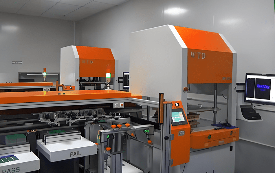
- Automated production lines: automation raises consistency and removes human error from steps where a few microns matter.
- PTFE-experienced lamination: soft, low-loss materials need dedicated press cycles and desmear chemistry — a standard FR-4 line will quietly damage them.
XCE PCB manufactures high-frequency boards from 2 to 72 layers, panels up to 600×1200 mm, with impedance held to ±10% and prototypes shipped in as fast as 24 hours.
Key Point 5: Surface Treatment
Proper surface finish improves solder reliability and prevents oxidation. For RF boards the flatness of the pad matters as much as the chemistry:
| Surface finish | What it provides | Best suited for |
|---|---|---|
| ENIG | Flat pad geometry, excellent solderability, industry default for RF pads | Most high-frequency boards |
| ENEPIG | Adds a palladium layer for extra robustness over nickel | Wire-bondable pads and extremely high-frequency assemblies where signal integrity is critical |
The choice depends on the assembly process and frequency band — we recommend the finish together with the stackup, not as an afterthought.
Key Point 6: Reliability Testing and Quality Control
Environmental and reliability verification is essential before any high-frequency board ships:
- Thermal cycling: simulates temperature fluctuation to confirm the laminate, plating, and solder joints stay stable.
- Humidity testing: verifies performance in high-humidity environments — critical for the low-moisture-uptake materials specified above to actually deliver in the field.
- Routine inspection: electrical performance checks and physical damage assessment catch potential issues before the board reaches the customer.
- Usage-environment monitoring: temperature, humidity, and chemical exposure in the end application should feed back into the acceptance criteria, not just the datasheet.
Common Production Pitfalls We Watch For
Considerations that separate a qualified RF fabricator from a general one:
- Treating RF material like FR-4: wrong desmear or press parameters cause warpage, delamination, and inconsistent Dk.
- Skipping coupon-based impedance verification: simulation is not a substitute for measured coupons per panel.
- Ignoring environmental testing: boards for outdoor, automotive, or medical use fail late and expensively without early thermal and humidity validation.
- Under-specified maintenance and storage: finished boards need controlled storage and handling to preserve surface finish quality until assembly.
Conclusion
High-frequency high-performance PCB production is a chain: material selection, impedance-driven layout, disciplined manufacturing, and verification testing. Every link needs attention and precision — and every link is easier when your fabricator is involved before the stackup is frozen. If you have a design moving into production, send us your stackup and frequency band; our engineers will review manufacturability and return a quote with the process plan attached.
Frequently Asked Questions
What materials are used for high-frequency high-performance PCBs?
Why is impedance control so critical in high-frequency PCB production?
What surface finish is best for high-frequency PCBs?
How do you verify reliability before shipping?
How fast can you produce high-frequency PCB prototypes?
Planning a High-Frequency PCB Build?
Send us your Gerber files and requirements for a manufacturability review and a tailored quotation.
sales1@xcepcb.com
+86 180 3818 8537