
PCB surface treatment processes are usually presented as a list of names, and that is where the trouble starts. A fabricator quotes “immersion gold”, another quotes “gold”, a third quotes “hard gold”, and the three are not the same finish at any level: one is 0.05 µm of gold over nickel, one is 1.5 µm of a gold-cobalt alloy over electrolytic nickel, and a thirty-fold difference in gold thickness sits behind a single word. This guide treats the finish as what it actually is — a specified deposit with a floor, a ceiling, a shelf life and one characteristic failure mode — and gives the thickness windows from IPC-4552, 4553, 4554, 4555 and 4556, the cost each option adds, and the assembly requirement that should decide the choice.
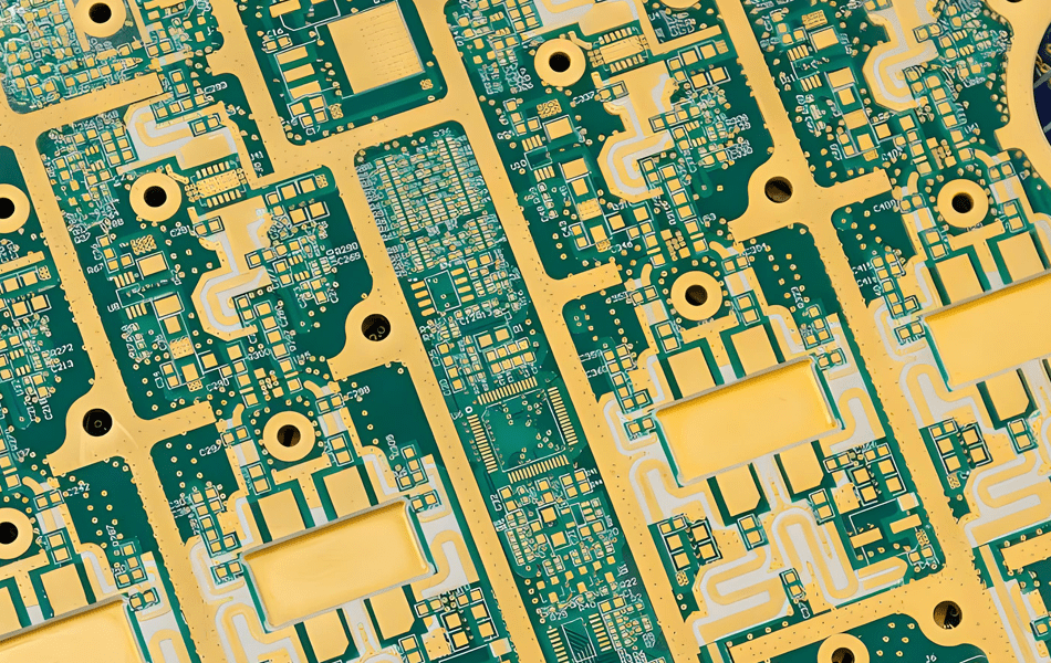
Ten Headings, Seven Finishes: Why the Names Fail
The first thing to fix is vocabulary, because the original version of this article — like most finish lists on the internet — contained ten headings of which only seven are solderable metal deposits. Two of the ten were the same process described twice, and three were not surface finishes at all.
| Heading as commonly written | What it actually is |
|---|---|
| Hot air solder leveling (HASL) | A finish: molten SnPb or SAC305 blown flat with air knives, 1–40 µm, uneven by nature |
| OSP | A finish: a 0.2–0.5 µm organic azole film bonded to bare copper, not a metal at all |
| ENIG | A finish: electroless Ni-P 3–6 µm plus immersion gold 0.05–0.10 µm |
| “Sinking tin” | A finish: immersion tin. “Sinking” is a machine translation of the Chinese term for immersion tin, and it appears in English quotations often enough to cause confusion |
| Immersion silver | A finish: 0.12–0.40 µm of silver displacing copper |
| ENEPIG | A finish: Ni-P, then electroless palladium, then immersion gold |
| Hard gold (EHG) | A finish, but electrolytic: it needs a plating bus and cannot be applied to an isolated pad |
| “Chemical tin-silver plating (ENEPIG)” | A duplicate of ENEPIG in the same list. There is no electroless tin-silver finish in production; the two real processes are immersion tin and ENEPIG |
| Laser marking | Not a finish. It is marking, applied over solder mask, and it changes nothing about solderability |
| Carbon ink / peelable blue mask | Not finishes. Carbon ink is a functional coating for keypads, bleed resistors and shielding contacts; peelable mask is temporary protection that is removed before assembly |
This matters commercially, not just editorially. When a purchase order says “gold”, the supplier can legitimately deliver ENIG with 0.05 µm of gold, or hard gold with 1.5 µm — a thirty-fold difference in gold, two different deposition chemistries, and a wear life that differs by three orders of magnitude. The rest of this article therefore works from deposit, thickness and standard, because those are the only things that can be inspected.
The Eight Finishes and What Each One Deposits
Eight processes cover essentially every board in production. Two adjacent options are included because they appear in quotes without being named: nickel-free palladium finishes for millimetre-wave work, and soft gold for chip-on-board.
| Finish | Deposit and thickness | Governing document | Where it earns its place |
|---|---|---|---|
| HASL, lead-free | SAC305 (or SnCu), 1–40 µm, dome-shaped | J-STD-003 for solderability | Through-hole boards, 0.65 mm pitch and coarser, lowest cost |
| OSP | Organic azole on copper, 0.2–0.5 µm | IPC-4555 | High-volume single-pass assembly with a short fabrication-to-build window |
| Immersion silver | Ag on Cu, 0.12–0.40 µm (typical 0.2–0.3) | IPC-4553A | Flat pads at low RF loss, cost below the gold finishes |
| Immersion tin | Sn on Cu, 1.0 µm minimum (1.15–1.3 typical) | IPC-4554 | Press-fit and flat pads with a known six-month consumption plan |
| ENIG | Ni-P 3.0–6.0 µm (P 7–10 wt%) + Au 0.05–0.10 µm | IPC-4552B | Fine pitch, long storage, solder plus contact in one finish |
| ENEPIG | Ni-P 3.0–6.0 + Pd 0.05–0.15 + Au 0.03–0.07 µm | IPC-4556 | Solder and wire bond on the same pad; higher reflow count |
| EPIG / DIG (nickel-free) | Pd 0.1–0.2 + Au 0.03–0.05 µm (EPIG); gold directly on copper (DIG) | No settled industry document — specify your own window | Above roughly 20 GHz, where the nickel layer is the loss; and bondable |
| Hard gold | Electrolytic Ni 2.5–5 µm + Au-Co or Au-Ni 0.76–1.5 µm, 130–200 Knoop | ASTM B488, MIL-G-45204 | Edge connectors and contacts with hundreds to thousands of mating cycles |
| Soft / flash gold | Electrolytic Ni + Au at 99.9 % purity, 0.1–0.5 µm | MIL-G-45204 purity classes | Gold wire bonding, chip-on-board |
One structural point sits underneath the table: every finish above except OSP and carbon ink is a metal stack, and every metal stack has a barrier layer and a protective layer that do different jobs. In ENIG the nickel is the barrier and the solderable surface; the gold exists only to keep the nickel from oxidising in storage, and it dissolves into the solder within about two seconds at reflow temperature. Once that is clear, three otherwise puzzling facts make sense: why gold thickness is capped, why nickel thickness decides the RF loss, and why black pad is a nickel problem that shows up as a gold surface.
Every Finish Has a Floor and a Ceiling
Finish specifications are windows, not minimums, and the upper limit is usually the more interesting number. Each of the last three revisions of these standards added one, because the industry kept discovering that more metal is not better.
| Finish | Specified window | What the ceiling prevents |
|---|---|---|
| ENIG | Ni 3.0–6.0 µm, Au 0.05–0.10 µm, P 7–10 wt% | Gold above about 0.10 µm makes the joint brittle and can hide a corroded nickel surface under a cosmetically perfect pad |
| ENEPIG | Ni 3.0–6.0, Pd 0.05–0.15, Au 0.03–0.07 µm | Excess gold defeats the palladium barrier and reopens the black-pad route the palladium was added to close |
| Immersion silver | 0.12–0.40 µm at ±4σ, typical 0.2–0.3 | Thicker silver does not solder better; it costs more and gives more metal for migration |
| Immersion tin | ≥1.0 µm at −4σ, typical 1.15–1.3 | This one is a floor, not a ceiling: the tin is consumed from below by copper-tin intermetallic growth |
| OSP | 0.2–0.5 µm by supplier window; no enforceable industry thickness limit | Nothing measurable — which is why the thickness has to go on the purchase order |
| Hard gold | ≥0.76 µm (30 µin); 1.27–1.5 µm for high-reliability contacts | Hardness comes from the cobalt or nickel codeposit, purity from the bath; one without the other fails either wear or contact resistance |
The verification detail matters as much as the window. XRF reads thickness on a pad of roughly 2.25 mm², the numbers are quoted at ±4σ from the process mean, and the actual criterion is statistical — a supplier measuring a single point on one coupon is not demonstrating a process. Ask for the per-lot certificate with the measurement pad size stated, and for ENIG also the phosphorus content, because 7–10 wt% is the range that keeps the nickel both corrosion-resistant and solderable.
Thickness Is an Electrical Parameter
On a high-frequency board the finish is not a coating over the conductor, it is part of the conductor. Current flows in the outer skin of the deposit, and how deep that skin is compared with the thickness decides whether the finish is electrically transparent.
| Metal | δ at 1 GHz | δ at 10 GHz | δ at 28 GHz | Surface resistance vs copper |
|---|---|---|---|---|
| Copper | 2.06 µm | 0.65 µm | 0.39 µm | 1.00 |
| Silver | 2.00 | 0.63 | 0.38 | 0.97 |
| Gold | 2.49 | 0.78 | 0.47 | 1.21 |
| Nickel | 4.20 | 1.33 | 0.79 | 2.04 |
| Tin | 5.25 | 1.66 | 0.98 | 2.55 |
Read the gold row against the ENIG window. A 0.05–0.10 µm gold layer is eight to fifteen times thinner than the skin depth in gold at 10 GHz, so it carries almost no current at RF; it is a storage protection that dissolves in the solder, exactly as intended. The nickel beneath it, at 3–6 µm, is two to five times thicker than the skin depth in nickel — which means the current is fully inside the nickel, and the conductor loss is set by a metal with twice the surface resistance of copper. That is the whole RF case against ENIG, and it is a thickness argument, not a materials argument.
The practical ranking follows directly: OSP and immersion silver sit closest to bare copper, ENIG and ENEPIG add a nickel layer, immersion tin adds a thicker and lossier metal, and HASL adds an uneven 1–40 µm of tin on top of everything. On a 0.254 mm stack at 10 GHz the difference between ENIG and a nickel-free finish is of the order of 0.1–0.15 dB per inch, rising to 0.2–0.3 dB per inch at 28 GHz; the estimate comes from the surface-resistance ratio, so it should be confirmed on a coupon rather than quoted as a guarantee.
The nickel-free finishes exist for that gap. EPIG deposits palladium directly on copper with a thin gold flash, and DIG deposits gold directly on copper; both remove the 3–6 µm of nickel that dominates the loss above roughly 20 GHz, and both remain bondable. They cost more, have shorter bath life and are far less widely available, which is why they are specified for millimetre-wave and bonding work rather than as a general upgrade. The electrical treatment of this subject, including what the nickel costs in a link budget, is worked through in surface treatment on high-frequency PCB.
Flatness Is What the Assembler Is Buying
For everything below about 3 GHz, the finish choice is decided by assembly geometry rather than by loss. HASL leaves domes: the air knife flattens the solder but cannot make it planar, and the resulting height variation is measured in several micrometres across a pad. On a 0.65 mm pitch that is harmless. On a 0.4 mm pitch BGA, where the ball is around 0.25 mm and the paste deposit is 0.1 mm thick, a dome under the pad changes the stand-off height, and stand-off height is what decides whether the joint survives thermal cycling.
- 0.65 mm pitch and coarser: HASL is fine, and it is the cheapest finish that exists.
- 0.5 mm and below: a flat finish — ENIG, ENEPIG, immersion silver, immersion tin or OSP. The choice among them then comes from storage, bonding and RF, not from flatness.
- QFN and any large thermal pad: flatness plus paste control. A thermal pad with 25 % voiding runs 15–20 °C hotter at the junction; the finish contributes to that only through coplanarity, but it is the first thing to check when voiding appears.
Two secondary properties are worth naming because they are invisible in a finish comparison table. OSP is flat but not probe-friendly: a test probe penetrates the film and leaves exposed copper that oxidises before the board reaches assembly, so boards with in-circuit test points are usually specified ENIG or hard gold at the points. Immersion tin is flat but soft, and repeated probing or handling marks it; the marks are cosmetic until they are not, because a scratched tin surface re-oxidises and stops wetting.
One Failure Mode per Finish
Each of these processes has a characteristic way of failing, and the failure is nearly always a process-window problem rather than a materials problem. Knowing which one applies is what turns a finish choice into an inspection plan.
| Finish | Characteristic failure | Mechanism | What to inspect |
|---|---|---|---|
| HASL | Thermal shock and non-planarity | 250–260 °C dip, then air-knife cooling; solder wicks into holes and onto adjacent features | Coplanarity, hole fill, pad lift on thin laminates |
| OSP | Wetting loss after storage or handling | The azole film degrades with heat, humidity and fingerprints; it survives a limited number of reflows | Wetting balance after the specified storage period |
| Immersion silver | Sulfide tarnish, creep corrosion, silver migration | Ag2S forms in sulfur-bearing air and packaging; under bias and humidity silver migrates and grows dendrites | Colour and XRF, surface insulation resistance, packaging audit |
| Immersion tin | Solderability loss and whiskers | Cu6Sn5 grows from the copper side and consumes the free tin; compressive stress in the deposit grows whiskers | Intermetallic thickness, SEM per JESD22-A121, storage time |
| ENIG | Black pad | Hyper-corrosion of the nickel during the gold step leaves a phosphorus-rich, non-wettable layer | Nickel corrosion rating per IPC-4552B, ball shear, P content |
| ENEPIG | Bond lift when the palladium drifts | A three-layer bath is harder to hold; palladium below the window lets gold and nickel meet again | Pd thickness by XRF, wire pull and shear per lot |
| Hard gold | Wear-through and contact resistance | Gold too thin or too soft for the cycle count; nickel underlayer below 2.5 µm wears through first | Thickness on the finger, Knoop hardness, mating-cycle test |
| EPIG / DIG | Copper diffusion and oxidation | Without a nickel barrier, copper reaches the gold surface during high-temperature assembly | Gold thickness, bake test at assembly temperature, contact resistance |
Black Pad Is a Nickel Problem Wearing a Gold Surface
Black pad deserves its own section because it is the failure that most often turns a finish decision into a field return, and because it looks like a gold defect while being caused entirely by the nickel underneath.
The immersion gold step is a displacement reaction: gold ions in solution are reduced at the nickel surface while nickel dissolves. That is intentional and self-limiting — once the surface is covered, the reaction stops, which is why the gold layer is thin. If the bath is too active (temperature, pH, gold concentration, or simply bath age measured in metal turnovers), the reaction does not stop cleanly: the gold-nickel galvanic couple keeps corroding nickel through pores, and the nickel surface left behind is enriched in phosphorus to 20–30 at% instead of the 7–10 wt% of a healthy deposit. That phosphorus-rich layer is not solderable, and the joint that forms on it fractures between the nickel and the tin-nickel intermetallic — a brittle, low-force break that often only appears after thermal cycling, which is why it escapes incoming inspection.
- Specify the phosphorus window (7–10 wt%) and require it on the certificate. Low-phosphorus nickel corrodes faster; high-phosphorus nickel is harder to solder and more brittle.
- Cap the gold at 0.10 µm. Thick gold is not a premium; it is the condition under which the corrosion hides.
- Require a corrosion rating per IPC-4552B with an acceptance level written into the purchase order, rather than “no black pad” as a verbal promise.
- Control bath age through metal turnovers and require the fabricator to state the limit. This is the single variable most often left out of a supplier qualification.
ENEPIG was introduced substantially to close this route: the 0.05–0.15 µm palladium layer separates nickel from the gold bath, so the displacement reaction no longer reaches the nickel. It is why ENEPIG tolerates more reflows and why it is the usual answer for 0.4 mm pitch, Class 3 and any board that will be reworked. The trade is a third bath to control and roughly 50–100 % more finish cost.
Each Finish Runs on a Different Clock
Shelf life is a specification, not a marketing number, and it is set by the mechanism from the previous section. Boards bought on price and stored for a year routinely arrive at assembly with a finish that was correct when it shipped.
| Finish | Stated shelf life | What ends it | Storage that actually helps |
|---|---|---|---|
| HASL | 12 months | Oxide and intermetallic growth on the solder surface | Sealed with desiccant; re-solderable after long storage |
| OSP | 6 months, 3–6 in practice | Film degradation, humidity, handling | Vacuum foil, no fingerprints, FIFO discipline |
| Immersion silver | 6–12 months | Sulfide tarnish; sulfur in paper and packaging | Sulfur-free interleaving, sealed foil, controlled humidity |
| Immersion tin | 6 months | Intermetallic reaching the surface | Sealed, below 30 °C; do not bake before assembly |
| ENIG | 12 months and often more | Not the gold — corrosion that started in the plating bath | Dry, sealed; the gold surface itself is inert |
| ENEPIG | 12 months | Same as ENIG, plus palladium bath drift | Dry, sealed |
| Hard gold | Effectively indefinite | Nothing chemical; wear is mechanical | Protect the fingers from abrasion |
Two practical notes. Standard storage is 20–25 °C at 45–55 % relative humidity with a humidity indicator card in the bag, and the card matters more than the label because it is the only evidence at goods-in. And baking is not a universal rescue: it recovers moisture but degrades OSP, immersion silver and immersion tin, and it grows the intermetallic under tin. A board baked to dry it and then stored again has less margin than before it was baked.
Selective Finishes: Two Processes on One Board
Most boards with gold fingers do not have one finish; they have two. The connector area gets hard gold, everything else gets ENIG, OSP or immersion silver, and the boundary is where the problems are.
- Hard gold is electrolytic and needs a bus. Every finger must be connected to a common conductor during plating, and that bus is routed on the panel and then removed. Its removal is a mechanical operation next to finished plating, and it is worth asking who does it and how the edge is deburred.
- Masking needs room. The gap between a plated zone and a masked zone is typically 0.5–0.75 mm; below that, tape lift and bath bleed produce a ragged boundary and, worse, gold contamination in the electroless nickel bath.
- Two passes, two contamination paths. Gold drag-in to an electroless nickel bath causes black-pad-type defects across the whole panel, not just near the fingers, so a fabricator running both processes needs segregated lines and a drying step between them.
- The drawing must dimension the zones. “Hard gold on the fingers” is not a specification; a dimensioned zone with a thickness for each area is.
Selective finishing is also where cost control lives: hard gold over the full board can add a quarter of the board price, while hard gold on 8 mm of fingers at the edge is a small line item. The finishes themselves are covered per square metre in the next section, but the geometry is what decides whether the number is small or large.
PTFE and Hybrid Boards: Where the Rules Change
Everything above assumes an FR-4 substrate that tolerates the process. On PTFE laminates two of the eight finishes become questionable and one becomes mandatory.
HASL is the wrong process for PTFE. A 250–260 °C solder dip is a thermal shock into a material with a Z-axis expansion of 200–240 ppm/°C: on a 1.6 mm board crossing 215 K that is around 80 µm of expansion, three to four times what a high-Tg FR-4 does over the same range. The visible results are pad lift, barrel cracking at the knee and delamination at the copper interface; the invisible one is cold flow of the PTFE under the air knife, which thins the dielectric locally and moves the impedance of the very line the finish was supposed to protect. The general thermal behaviour is set out in glass transition temperature in PCB manufacturing.
OSP has nothing to bond to on the dielectric. It is a copper-azole bond, so it exists only where copper is exposed. On a PTFE board the RF launch pads are copper defined by the mask opening, which is fine — but any design that expects a finish to make a bare PTFE surface solderable is expecting something no finish does. PTFE surface energy is 18–20 mN/m, and a metal deposit has to be present before any solder will wet.
For RF work the shortlist is ENIG, immersion silver or OSP, with the choice driven by loss budget and shelf life rather than by solderability; above roughly 20 GHz a nickel-free finish is the only way to remove the nickel from the loss stack. Immersion silver is the usual compromise: closest to bare copper electrically, flat, and inexpensive relative to gold — with tarnish as the price, and tarnish that is largely cosmetic because silver sulfide is conductive enough that a thin film changes loss by very little, while creep corrosion in a humid sulfur environment is a real reliability issue rather than an RF one. The full electrical argument, including what nickel costs in a link budget and how each finish behaves at the launch, is in surface treatment on high-frequency PCB, and the process differences between the two material classes are in high-frequency PCB versus standard PCB.
What Each Finish Adds to the Price
Finish cost is quoted per square metre of plated area, and on a standard board it lands between 5 and 15 % of the price; the rest is laminate, drilling, imaging, solder mask and test. The figures below are indicative adders for a 4-layer 1.6 mm FR-4 board at panel quantity, and they should be treated as a ranking rather than a quotation.
| Finish | Adder per ft² | Adder per 100×100 mm board | When it is the wrong economy |
|---|---|---|---|
| HASL, lead-free | 0.15–0.25 USD | 0.02–0.04 USD | Fine pitch, thin laminate, PTFE |
| OSP | 0.10–0.20 | 0.01–0.03 | Long inventory, multiple reflows, heavy probing |
| Immersion tin | 0.15–0.30 | 0.02–0.05 | More than one reflow, storage beyond six months |
| Immersion silver | 0.25–0.45 | 0.04–0.07 | Sulfur-bearing or high-humidity environment |
| ENIG | 0.30–0.50 | 0.05–0.08 | Wire bonding, or above 20 GHz |
| ENEPIG | 0.45–0.75 | 0.07–0.12 | Plain SMT at 0.5 mm pitch with no bonding |
| EPIG / DIG | 0.40–0.70 | 0.06–0.11 | Anywhere nickel loss does not matter |
| Hard gold, selective | 0.60–1.50 | 0.10–0.25 | Applied to the whole board instead of the fingers |
The comparison that actually decides the choice is not the adder but the cost of getting it wrong. A finish delta of 0.03 USD per board on a 10,000-piece order is 300 USD; one rework loop on a single assembled board carrying a 200 USD FPGA costs more than that, and a field return costs an order of magnitude more. The cheap finishes are cheap for reasons that are documented in the standard — a six-month shelf life, a reflow limit, a tarnish mechanism — and those reasons are only harmless when the programme matches them.
Selection Matrix by Assembly Requirement
Start from what the board has to survive, not from what the last project used. Each row below is a requirement that narrows the choice to one or two finishes.
| Requirement | Finish | Why | Avoid |
|---|---|---|---|
| Through-hole, 0.65 mm pitch and coarser | Lead-free HASL | Cheapest, rugged, already solder-coated | Nothing below 0.5 mm pitch |
| 0.5 mm BGA, 12-month storage | ENIG | Flat, inert surface, solder and contact in one | HASL, OSP for long inventory |
| 0.4 mm pitch, three or more reflows, Class 3 | ENEPIG | Palladium blocks black pad and tolerates rework | ENIG at the thin end of its window |
| Gold or aluminium wire bonding | ENEPIG, or soft gold for gold wire | Bondable surface plus solderable periphery | Standard ENIG for aluminium wire |
| Press-fit connector | Immersion tin ≥1.0 µm, or ENEPIG | Thick, ductile, flat; survives insertion force | HASL and thin OSP |
| Edge connector, hundreds of cycles | Hard gold 0.76–1.5 µm over Ni ≥2.5 µm | Wear resistance from the alloy codeposit | ENIG, which wears through in tens of cycles |
| RF above 10 GHz, no bonding | Immersion silver or OSP | No nickel in the skin depth | ENIG with thick gold, HASL |
| RF above 20 GHz with bonding | EPIG or DIG | Nickel-free and bondable | Any nickel-bearing stack |
| Sulfur-bearing or humid environment | ENIG or ENEPIG | Gold surface is chemically inert | Immersion silver without packaging control |
| In-circuit test points | ENIG, or hard gold at the points | Repeated probing without breaking the surface | OSP, immersion tin |
What to Put on the Fabrication Drawing
A finish callout that cannot be inspected is not a specification. Six items close the gap between what was intended and what was plated.
| Item | What it must state | What it prevents |
|---|---|---|
| Finish and standard | Name plus the revision of the IPC or ASTM document, not just “gold” | ENIG quoted and hard gold delivered under the same word |
| Thickness window | Floor and ceiling per layer, measurement method, and the pad size used for XRF | A single-point measurement presented as a process |
| Chemistry limits | Phosphorus content for ENIG and ENEPIG, plus the acceptable nickel corrosion rating | Black pad discovered after assembly rather than at goods-in |
| Selective zones | Dimensioned areas, thickness per area, masking gap, and how the plating bus is removed | Gold bleed into the nickel bath and a ragged boundary |
| Shelf life and packaging | Stated shelf life, vacuum foil, desiccant, humidity indicator, sulfur-free interleaving for silver | A correct finish that is unusable by the time it is assembled |
| Coupon requirements | Per-lot XRF thickness, wetting balance, ionic contamination, and where the coupon sits on the panel | No way to prove any of the above after the fact |
The ionic contamination item connects this page to the assembly side: a finish and the flux that removes its oxide are a system, and residues left on the surface are a dielectric layer nobody measured. The chemistry and the cleanliness test methods are in soldering oils and fluxes in PCB manufacturing.
Six Claims Worth Correcting
The version of this article that ranked for this page before the rewrite contained a finish list and no specifications. These are the statements in it that do not survive a review, and the correction for each.
| Claim | What is actually true |
|---|---|
| “Chemical tin-silver plating” listed as a separate process | It is ENEPIG described a second time in the same list, under a name that does not correspond to any production finish. There is immersion tin and there is ENEPIG; there is no electroless tin-silver |
| “Sinking tin” | Immersion tin, IPC-4554, minimum 1.0 µm. The thickness is a floor because copper-tin intermetallic growth consumes the deposit during storage |
| “Laser marking is a surface treatment” | It is marking over solder mask. It has no bearing on solderability, corrosion or contact resistance, and it belongs in a marking specification |
| “Carbon ink or peelable mask as surface treatment” | Carbon ink is a functional coating for keypads, bleed resistors and shielding contacts; peelable mask is temporary protection removed before assembly. Neither is a solderable finish |
| “Immersion silver suits high frequency because silver conducts well” | The conductivity advantage over copper is 3 %; the real advantage is that there is no nickel layer. A nickel-bearing finish is roughly twice the surface resistance of copper, which is what actually shows up in the loss |
| “HASL is suitable for a variety of soldering processes” with no qualification | True at 0.65 mm pitch and coarser on FR-4. It is unsuitable for fine pitch, and on PTFE the 250–260 °C dip is a thermal and mechanical risk to the laminate itself |
There is a pattern in these: the original list treated finishes as brands rather than as deposits. Every correction above resolves to a number — a thickness, a phosphorus content, a reflow count, a shelf life — because those are the only terms on which a finish can be bought, inspected and rejected.
Conclusion
Choosing a PCB surface treatment is a four-variable problem: what the assembly needs (pitch, bonding, insertion force), what the environment will do to the surface (sulfur, humidity, cycles), how long the board will sit before it is built, and what loss the design can afford. Any finish that satisfies all four is a correct answer, and the cheapest one that does is the right one.
The failure mode of the whole subject is specification by adjective. “Gold”, “lead-free” and “high reliability” are not finish specifications; “ENIG per IPC-4552B, Ni 3–6 µm, Au 0.05–0.10 µm, P 7–10 wt%, corrosion rating per agreed level, 12-month shelf life, vacuum packed with humidity indicator” is one, and it can be measured, argued about and rejected.
XCE PCB plates ENIG, ENEPIG, immersion silver, immersion tin, OSP and selective hard gold on high-frequency and mixed-material builds: 2 to 72 layers, impedance ±10 %, panels to 600×1200 mm, samples in as fast as 24 hours, inspected to IPC-A-600G and IPC-6015. Every order leaves with the finish certificate and the coupon data attached, because the numbers in this article are only worth anything if they are on paper. The fabrication sequence around the finish is in the twelve-step manufacturing overview, and the plating stages that precede it are in plating in high-frequency PCB manufacturing.
Frequently Asked Questions
What are the main PCB surface treatment processes?
How thick should ENIG gold be?
Does the surface finish affect insertion loss?
Why does immersion tin have a minimum thickness instead of a maximum?
What is black pad and how do I prevent it?
Can I use HASL on a PTFE high-frequency board?
Need a Finish Callout That Survives the Quote Cycle?
Send us your Gerber files and requirements for a manufacturability review and a tailored quotation.
sales1@xcepcb.com
+86 180 3341 4657