
Learn why high frequency PCB prototyping is critical before mass production. Discover how RF PCB prototyping helps verify design performance, reduce manufacturing defects, optimize costs, and evaluate PCB supplier capabilities.
Why High Frequency PCB Prototyping Is Essential Before Mass Production
High Frequency PCB Prototyping is a critical step in the development and manufacturing of RF, microwave, radar, satellite communication, and 5G circuit boards. Before moving into full-scale production, engineers and manufacturers need to verify that the design performs as expected and that the manufacturing process can consistently meet technical requirements.
Many companies view PCB prototyping as an additional expense. In reality, a well-executed high frequency PCB prototype can save significant time, cost, and risk during mass production. It allows potential issues to be identified and corrected early, preventing expensive failures after production has already begun.
For high frequency PCB projects, where impedance control, dielectric properties, insertion loss, and dimensional accuracy are critical, prototyping is not optional—it is an essential part of the development process.
One of the most important reasons for high frequency PCB prototyping is to evaluate the actual manufacturing capabilities of a PCB supplier.
When working with a new PCB manufacturer, specifications and certifications alone do not always reflect real production capability. A prototype build provides direct evidence of the supplier’s engineering expertise, process control, and ability to meet technical requirements.
Through prototyping, customers can evaluate:
Manufacturing quality
Impedance control capability
Registration accuracy
Copper plating quality
Surface finish consistency
Material handling expertise
RF PCB fabrication experience
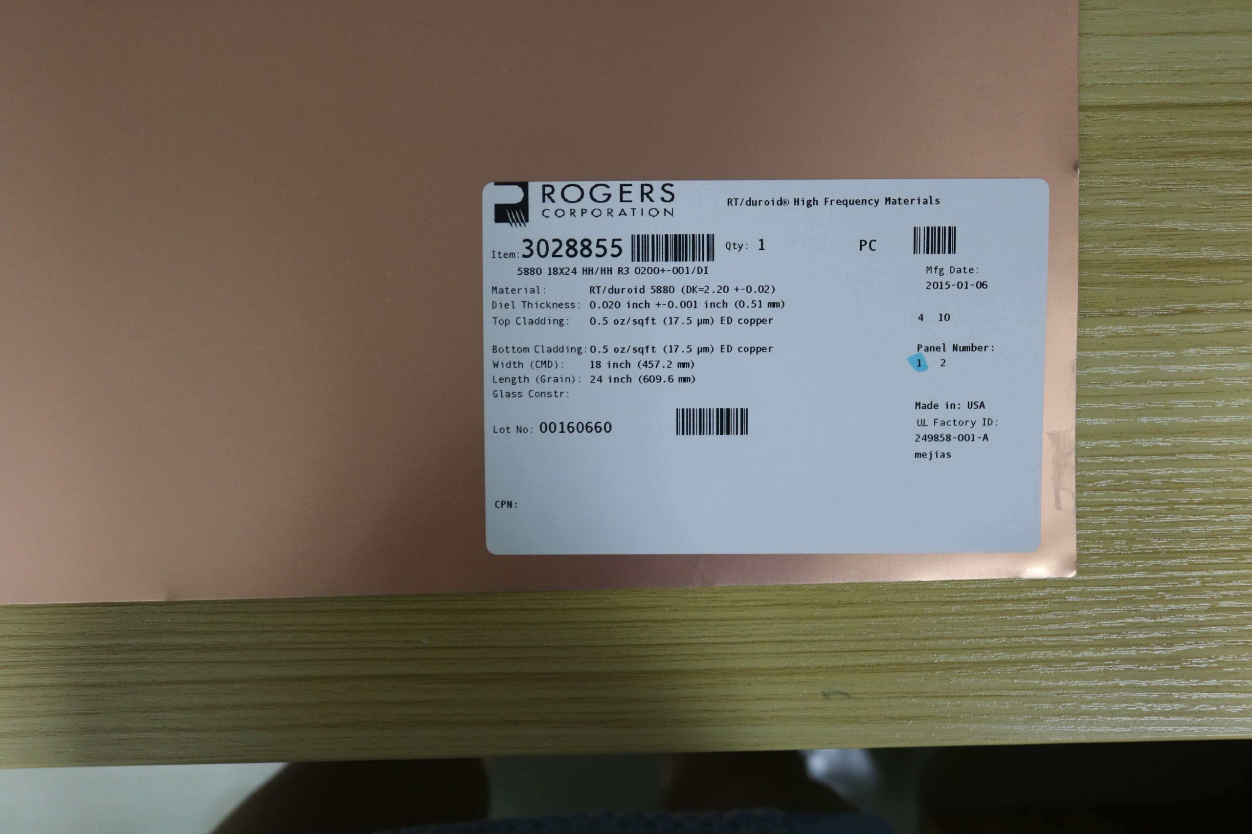
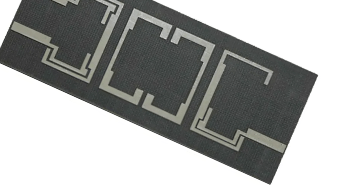
For high frequency materials such as Rogers RO4350B, RO4003C, RT5880, RO3003, and PTFE laminates, production experience is especially important because these materials require specialized processing methods.
A successful prototype demonstrates that the manufacturer can reliably support future production requirements.
Related Reading:
https://szxcepcb.com/product-category/4/
Reduce Defects During Mass Production
Another major benefit of high frequency PCB prototyping is the reduction of production defects.
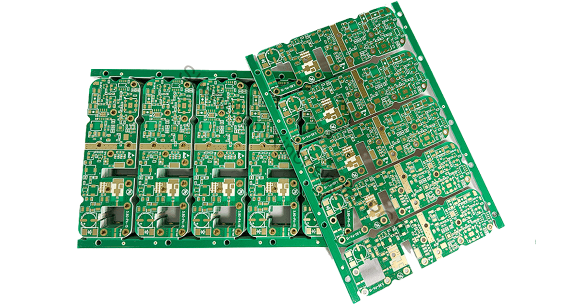
High frequency PCBs often involve:
Controlled impedance structures
Tight tolerance drilling
Multilayer lamination
PTFE processing
RF signal routing
High-density layouts
Because of this complexity, even a small design or manufacturing issue can create significant problems during volume production.
By producing a prototype first, engineers can perform comprehensive testing and validation before releasing the design for mass manufacturing.
Typical prototype verification includes:
Electrical testing
Impedance measurement
Signal integrity analysis
Insertion loss evaluation
Thermal performance testing
Mechanical dimension inspection
Any issues discovered during prototyping can be corrected before larger production quantities are manufactured.
This significantly reduces scrap rates, rework costs, and project delays.
Build a Strong Foundation for Future Production
High frequency PCB prototyping is also an important step in preparing for successful long-term production.
A prototype allows engineers to:
Verify circuit functionality
Evaluate RF performance
Confirm material selection
Optimize stackup design
Refine manufacturing processes
Estimate production costs
This early-stage validation helps identify opportunities for improvement before committing to large material purchases and production schedules.
For example, prototyping may reveal:
Alternative material options
Better layer stackup configurations
Improved impedance structures
More efficient panel utilization
Reduced manufacturing costs
These improvements can have a significant impact on both product performance and profitability.
Related Resource:
https://szxcepcb.com/company-profile/
Improve Product Reliability
Reliability is especially important in applications such as:
5G communication systems
Automotive radar
Aerospace electronics
Satellite communication
Military and defense equipment
Industrial RF systems
A prototype allows engineers to validate performance under real-world operating conditions before production begins.
Testing may include:
Temperature cycling
Environmental testing
Signal stability verification
Mechanical stress evaluation
Long-term reliability analysis
The data collected during prototyping helps ensure the final product will perform consistently throughout its service life.
Optimize Communication Between Customer and Manufacturer
Successful high frequency PCB fabrication requires close collaboration between the customer and the PCB manufacturer.
Before prototyping begins, both parties should clearly define:
Material specifications
PCB thickness
Copper weight
Controlled impedance requirements
Surface finish selection
Layer stackup
Frequency range
Mechanical tolerances
The prototyping stage provides an opportunity to verify that all technical requirements have been correctly interpreted and implemented.
This communication helps avoid misunderstandings and creates a smoother transition into mass production.
Why High Frequency PCB Prototyping Is Worth the Investment
While prototyping adds a small upfront cost, it often saves significantly more money in the long run.
Benefits include:
Lower manufacturing risk
Reduced defect rates
Improved product reliability
Faster production ramp-up
Better supplier qualification
More predictable production costs
For high frequency PCB projects, the cost of identifying and correcting a problem during prototyping is dramatically lower than discovering the same issue after hundreds or thousands of boards have been produced.
Why Choose SZXCEPCB for High Frequency PCB Prototyping
At SZXCEPCB, we specialize in high frequency PCB prototyping and production for RF and microwave applications.
Our capabilities include:
Rogers PCB fabrication
PTFE PCB manufacturing
RT5880 and RO3003 processing
Hybrid Rogers + FR4 stackups
Controlled impedance verification
TDR testing
IPC Class 2 and Class 3 manufacturing
Prototype and volume production support
Prototype lead time:
5–7 working days
No minimum order quantity
Our engineering team reviews every project to ensure manufacturability, performance, and cost optimization before production begins.
External Resources:
Rogers Corporation:
https://rogerscorp.com
IPC International:
https://www.ipc.org
Microwave Journal:
https://www.microwavejournal.com