
Dk 3.00 ± 0.04 · Df 0.0010 @ 10 GHz · ceramic-filled PTFE with no woven glass — where RO3003 boards belong, how they are actually built, and the five process points that decide your yield.
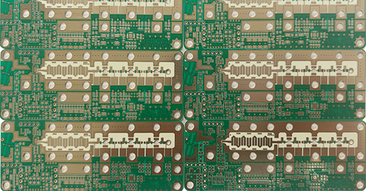
The Short Answer
Rogers 3003 (RO3003) is a ceramic-filled PTFE laminate built for circuits where phase stability and insertion loss at millimeter-wave frequencies decide whether the product works at all. It gives you a tightly held Dk of 3.00 ± 0.04, a dissipation factor of 0.0010 at 10 GHz, and — because there is no woven glass — none of the fiber-weave Dk variation that upsets phase-sensitive designs.
The trade-off is fabrication. PTFE does not behave like FR-4: it is soft, chemically inert, and smears when drilled, so hole preparation, lamination and plating all need dedicated process control. This guide covers where RO3003 boards are used, how XCE PCB builds them step by step, and the considerations that separate a clean build from a marginal one.
What Is Rogers 3003?
RO3003 belongs to the Rogers RO3000 family: a PTFE matrix loaded with randomly distributed ceramic filler, supplied without glass reinforcement. The ceramic loading raises the Dk from neat PTFE’s ~2.1 to 3.00 while keeping PTFE’s exceptionally low loss, and the absence of glass fabric removes the periodic Dk ripple that woven laminates impose on fine-pitch mmWave lines.
| Property (typical) | RO3003 |
|---|---|
| Resin system | PTFE + ceramic filler, no woven glass |
| Dk @ 10 GHz | 3.00 ± 0.04 |
| Df @ 10 GHz | 0.0010 |
| Moisture absorption | 0.06% |
| Thermal conductivity | 0.50 W/(m·K) |
| CTE, X/Y axis | 17 ppm/°C |
| CTE, Z axis | 25 ppm/°C |
| Standard thickness / copper | 0.127–1.524 mm (5–60 mil) · ½ oz–2 oz |
A Z-axis CTE of 25 ppm/°C is close to copper’s 17 ppm/°C, which is why RO3003 plated through-holes survive wide thermal swings better than most high-Tg FR-4 builds. For the material’s electrical behaviour in more depth, see our Rogers RT/duroid 3003 advantages overview.
Where Rogers 3003 Boards Are Used
RO3003 shows up wherever the link budget is tight and the phase has to stay put across temperature:
| Application | Band | Why RO3003 |
|---|---|---|
| Automotive radar (ADAS) | 76–81 GHz | Lowest loss and no fiber weave → stable phase per channel |
| Satellite comms PA / LNA modules | Ku / Ka | 0.06% moisture uptake keeps Dk drift small in humid ground terminals |
| Airborne and shipborne radar | X / Ku | Dk stability across −55 to +150 °C operating envelopes |
| Microwave point-to-point links | 18–40 GHz | Low insertion loss stretches hop distance |
| Phased-array antennas | mmWave | Uniform Dk across the panel keeps element-to-element phase matched |
| Test & measurement probes | DC–110 GHz | Tight lot-to-lot Dk tolerance supports calibration substrates |
In every one of these cases the material is chosen for the same reason: the dielectric has to stay constant, not just be low-loss on the datasheet.
The Fabrication Process, Step by Step
Building a RO3003 board means adjusting every step that touches an interface. Here is the sequence XCE PCB runs for PTFE laminates:
Step 1 — Surface Activation Before Patterning
PTFE is chemically inert: standard chemical cleaning cannot create a bondable surface. Before pattern transfer, copper surfaces and future hole walls go through sodium-naphthalene etching or plasma treatment, which micro-roughens the PTFE and leaves it receptive to photoresist and to the electroless copper that follows. Skip or under-run this step and nothing downstream can compensate — adhesion failures show up later as delamination or hole-wall pullaway.
Step 2 — Fine-Line Etching with Undercut Control
Once the pattern is transferred, the copper is etched. RO3003’s relative softness makes undercut the main risk: over-etch narrows the trace and shifts impedance, which on a 0.2 mm pitch mmWave line is enough to break the design. Etch compensation is applied per layer, and cross-sections are taken on the first panel of a lot rather than the last.
Step 3 — Lamination and Drilling
Multilayer RO3003 builds use PTFE-compatible bonding film (the Rogers 3001 film family) rather than ordinary FR-4 prepreg, with a lamination cycle matched to the PTFE melt behaviour — PTFE flows above its melting range, so over-temperature cycles deform the dielectric and detune the circuit.
Drilling is the second hazard. PTFE is ductile, so the bit smears material rather than cutting it cleanly, leaving a gum-like residue on the hole wall. That smear must be removed by plasma desmear or a PTFE-specific chemical desmear before plating; standard permanganate desmear designed for epoxy does not dissolve it.
Step 4 — Hole Metallization
This is where RO3003 builds most often fail. Standard electroless copper may not initiate on an activated PTFE surface at all. Production options are an enhanced electroless copper process tuned for PTFE, or a PVD seed layer followed by electroplating. Either way the electrolytic copper must be uniform through the hole — thin spots at the hole middle become barrel cracks after thermal cycling.
Step 5 — Surface Finish and Profiling
Finish is chosen by application: ENIG for fine-pitch mmWave assemblies, ENEPIG where gold wire bonding is required, electrolytic hard gold for edge connectors and test fixtures. Routing uses sharp, PTFE-rated bits with reduced feed rates — a dull bit tears the soft laminate and leaves burrs that interfere with connectors.
Why PTFE Changes Everything Compared with RO4003C
Designers often compare RO3003 with RO4003C and assume both are ‘Rogers, so both are special process’. They are not. RO4003C is a hydrocarbon/ceramic thermoset and runs on a standard FR-4 line; RO3003 is PTFE and needs the dedicated flow above. That single chemistry difference explains most of the cost and lead-time gap between the two materials.
Put simply: choose RO4003C when FR-4-compatible processing and cost matter up to roughly 20 GHz, and RO3003 when mmWave phase stability and the lowest loss justify a PTFE line. Our RO4003C vs RO3003 comparison breaks the two down parameter by parameter, and the RO4350B production guide covers the mid-range option that bonds well to FR-4 in hybrid stacks.
Key Considerations Before You Release the Design
- Thin laminate handling. RO3003 is commonly used at 0.127–0.254 mm. At that thickness the panel is floppy and dimensionally mobile, so plan stiffeners, carriers or a hybrid stack-up — and expect the fabricator to ask about support tooling.
- Temperature discipline. PTFE softens and flows when its melting range is exceeded. Reflow profiles, rework cycles and lamination temperatures must stay inside the datasheet window; repeated rework does more damage on PTFE than on FR-4.
- Dedicated consumables. Bonding films, drill bits, desmear chemistry and plating baths specified for PTFE are not interchangeable with FR-4 equivalents. Mixed lines are where yield quietly disappears.
- Impedance budget from the real Dk. RO3003’s Dk is 3.00, not 4.2 — trace widths for a 50 Ω line are noticeably wider. Designs copied from an FR-4 stack-up without recalculating will miss impedance by a wide margin.
- Copper balance. Because there is no glass fabric to stabilise the laminate mechanically, large copper-free areas can distort during lamination. Symmetrical copper distribution reduces bow and twist.
Hand these five points to your fabricator before tooling starts. They are cheap to design around and expensive to discover in cross-section.
Impedance Control on RO3003
RO3003 is one of the easier materials to control impedance on, precisely because its Dk is uniform — no fiber-weave effect means a trace crossing the panel sees the same dielectric everywhere. The variables that remain are copper thickness after plating, etch compensation and the accuracy of the Dk value used in the field solver.
XCE PCB controls impedance to ±10% on Rogers laminates, verified with TDR coupons on the production panel rather than on a separate test vehicle, so the number reflects the board you actually receive. For mmWave designs we recommend specifying impedance per layer and including the coupon on the panel edge in the fabrication drawing.
Quality Checks Before Release
On PTFE builds we run the following before a lot ships:
- Micro-section of plated through-holes — plating thickness, barrel integrity, resin smear residue
- Peel strength after thermal stress, to confirm surface activation actually worked
- TDR impedance on panel coupons, compared against the stack-up model
- Thermal cycling (typically −55 to +125 °C) with resistance monitoring for via integrity
- Ionic contamination and solder-mask adhesion checks where mask is applied
Surface activation failures are the ones that cost the most, because they pass visual inspection and fail in the field. Cross-sections and peel tests are the only reliable early warning.
Why Build Rogers 3003 with XCE PCB
XCE PCB has fabricated high-frequency laminates since 2009 — 2 to 72 layers, impedance controlled to ±10%, panel format up to 600 × 1200 mm, in a 5,000 m² facility staffed by 80+ engineers with more than 10,000 delivered projects behind them. PTFE processing (plasma desmear, PTFE-specific plating, controlled lamination) runs alongside a standard FR-4 line, so hybrid RO3003/FR-4 stack-ups are built and verified under one roof.
Prototypes can ship in as fast as 24 hours when the material is in stock. Send your stack-up and we will come back with an impedance model, a process note on the PTFE steps and a firm lead time — contact us here.
Conclusion
Rogers 3003 is not a difficult material to design with — it is a difficult material to fabricate without experience. The electrical case is straightforward: Dk 3.00 with 0.0010 loss and no glass weave gives the phase consistency that 77 GHz radar and mmWave links demand. The engineering case rests on five steps: activate the surface properly, control undercut, laminate and drill within the PTFE window, desmear before plating, and finish with tooling that respects a soft laminate.
Get those right and RO3003 delivers repeatable performance lot after lot. Get them wrong and you find out months later, in the field. That is the reason to build PTFE boards with a fabricator who runs a dedicated line.
Frequently Asked Questions
Is Rogers 3003 the same as RO3003?
Is RO3003 PTFE or hydrocarbon ceramic?
Why does RO3003 need plasma or chemical desmear before plating?
Can RO3003 be combined with FR-4 in a hybrid multilayer?
What thicknesses and copper weights are available for Rogers 3003?
How fast can XCE PCB deliver Rogers 3003 prototypes?
Building a Rogers 3003 Board? Talk to a PTFE Specialist
Send us your Gerber files and requirements for a manufacturability review and a tailored quotation.
sales1@xcepcb.com
+86 180 3818 8537