
When engineers discuss gold fingers on high frequency boards they usually describe them as a guarantee of continuity — a smooth plated interface that lets the signal leave the board without reflection. The electrical truth is the opposite and more useful: a gold finger is a wide pad, a wide pad is a low impedance, and the finger region is therefore a deliberate discontinuity that has to be contained rather than eliminated. What decides whether the board works is where that discontinuity begins and ends, whether the return current has a finger of its own to travel on, and how the plating stack was specified.
1. What the Finger Actually Is, Electrically
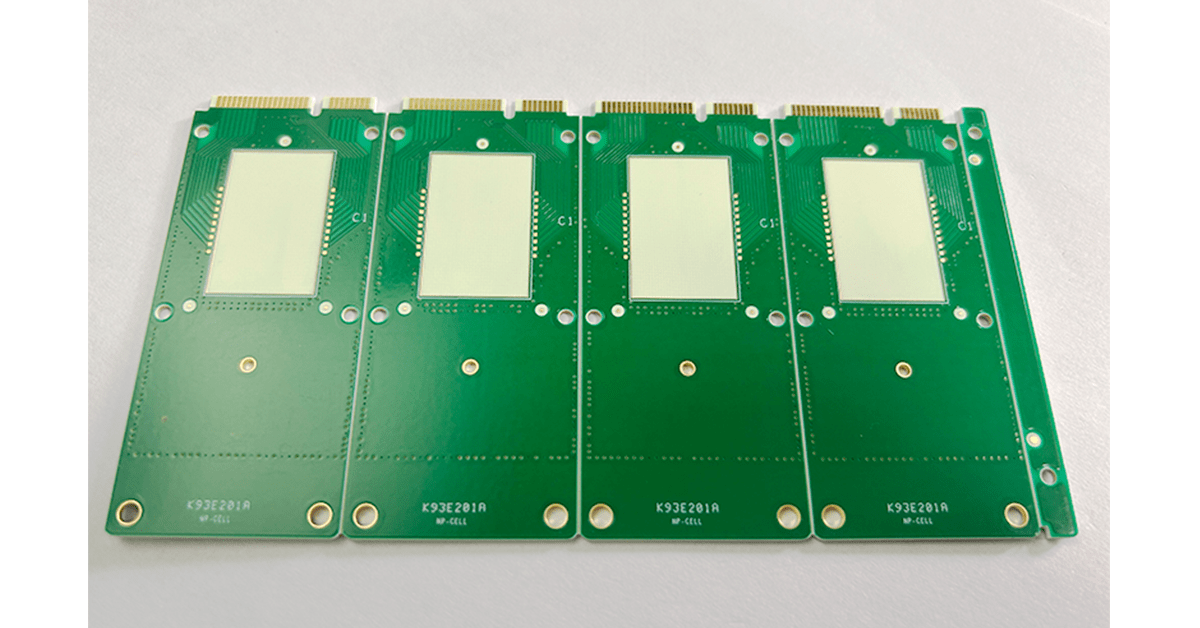
Strip the function down and a gold finger is a rectangle of copper at the board edge, plated with nickel and hard gold, that slides into a spring contact. It has three jobs that pull in different directions: carry signal with an acceptable reflection, carry current without overheating, and survive being inserted and removed. Only the first is a high-frequency problem, and it is the one most often solved by accident.
The reflection exists because impedance is set by geometry. A controlled 50 Ω microstrip on a 0.2 mm dielectric is about 0.47 mm wide. A finger that a connector can grip is one to three millimetres wide, because contact force, wear and alignment all want area. The same dielectric under a 2 mm pad presents roughly 18 Ω. That is not a defect; it is what the geometry says, and no plating thickness changes it.
| Finger width | W/h over a 0.2 mm dielectric | Approximate impedance | Where it is used |
|---|---|---|---|
| 0.5 mm | 2.5 | ≈48 Ω | Matched, but too narrow for a reliable contact |
| 1.0 mm | 5 | ≈30 Ω | Fine-pitch board-to-board |
| 2.0 mm | 10 | ≈18 Ω | DIMM and card-edge, the common case |
| 3.0 mm | 15 | ≈13 Ω | Power and hot-swap contacts |
Read the table as a budget. A 2 mm finger reflects roughly a quarter of the incident voltage at the boundary, and the only question is whether that reflection lands inside the connector or in the middle of the channel. Two rules follow: keep the trace at 50 Ω until it reaches the connector body, and taper over the shortest length the connector allows rather than over a convenient one.
2. The Return Path Needs a Finger Too
A signal finger without a ground finger is half a connection. The return current has to cross the same interface, and if it is forced to use a distant ground pin it makes a loop: inductance rises, the impedance at the transition collapses, and the pair radiates. At 10 GHz and above, this is usually the dominant mechanism at the connector, not the pad width.
The layout rules are unglamorous and well established. Put a ground finger immediately adjacent to every high-speed signal finger, and at both ends of any group of signals. Keep the same number of ground fingers as the connector provides, do not consolidate them into one large pad at the end, and make sure the ground fingers connect to a plane through multiple vias within a few millimetres of the edge — otherwise the finger is a stub, not a return. On a differential pair, the two fingers should be adjacent with a ground on each side, so the pair sees a symmetric environment and the intra-pair skew stays small.
The same geometry governs hot-swap power fingers, with a constraint added: the ground and power contacts must be sequenced so that ground mates first and breaks last, which is done with finger length rather than with electronics. That is a mechanical drawing decision, and it belongs with the connector datasheet on the table.
3. Plating: Electrolytic Hard Gold, and Why ENIG Cannot Substitute
The most common error in finger specifications is a sentence that contradicts itself: “gold fingers must use electrolytic nickel-gold (ENIG)”, followed two lines later by “ENIG must never be used for gold fingers”. Both cannot be true, and the resolution is that ENIG is not electrolytic. ENIG is electroless nickel, immersion gold: chemically deposited, 3–5 µm of nickel with 0.05–0.1 µm of gold on top. That gold is soft, thin and not intended to be worn.
| Finish | Stack | Hardness | Finger suitability | Note |
|---|---|---|---|---|
| Hard gold | Electrolytic Ni 2.5–5 µm + Au 0.76–1.27 µm | 130–200 HK | The only appropriate choice | ASTM B488 Type I, 99.7 % Au with 0.3 % Co or Ni |
| ENIG | Electroless Ni 3–5 µm + Au 0.05–0.1 µm | ≈90 HK | No — wears through in tens of cycles | Excellent for solderable pads, wrong for contacts |
| ENEPIG | Ni 3–6 + Pd 0.05–0.3 + Au 0.03–0.1 µm | ≈110–130 HK | Marginal | Buying wire-bond compatibility, not wear life |
| Immersion silver / OSP | 0.1–0.3 µm | n/a | No | No wear resistance at all |
Hard gold is an electroplating process, which has a design consequence that appears in layout rather than in chemistry: every finger needs a conductive path for the plating current. That is the “gold-plating lead” or bus bar, which is routed to the board edge and milled off after plating. A finger without a bus cannot be plated to thickness, and a bus that is not on the drawing is usually discovered as a plating thickness complaint.
Selective plating is the cost control: dry-film mask everything except the finger area, plate the whole panel, then strip. The consequence for high frequency is the nickel. Nickel is ferromagnetic, it has roughly twice the resistivity of copper and a skin depth of about 1.3 µm at 10 GHz — so a 2.5–5 µm underplate is a lossy layer several skin depths thick, sitting under the conductor at the exact place the channel is most sensitive. Where a finger must carry a millimetre-wave signal, the useful levers are a thinner nickel (within the wear requirement), a shorter finger, or a different transition altogether. How finishes compare as electrical layers rather than as coatings is covered in PCB surface treatment processes, and the electroless family specifically in electroless gold versus electroless silver.
4. Thickness Is a Wear Specification, Not a Luxury
Gold thickness on a finger is chosen against insertion cycles, and the industry tiers are narrow because the cost of gold is not. The published cycle figures vary with contact force, plating quality and the definition of failure, so treat the right-hand column as a band rather than a rating.
| Tier | Gold thickness | Nickel underplate | Insertion cycles, in practice | Typical use |
|---|---|---|---|---|
| Light duty | 0.25–0.4 µm (10–15 µin) | 2.5 µm | Tens to a few hundred | Prototype and test fixtures |
| Standard | 0.76 µm (30 µin) | 2.5–5 µm | ≈500–1,000 | DIMM, PCIe, card-edge |
| High reliability | 1.27 µm (50 µin) | 5 µm | Several thousand | Telecom, industrial, backplane |
| Extreme | 2.5 µm (100 µin) | 5 µm | Quoted up to 10,000 by some shops | Aerospace, defence, test sockets |
Two practical cautions. The first is that the wear mechanism is not linear in thickness: gold acts as a buffer that delays exposure of the nickel, and once nickel is exposed the contact resistance climbs quickly because nickel oxide is an insulator. The second is that thick gold over thin nickel fails at the nickel, not at the gold, so the underplate is not the place to economise. Where the finger meets a lead-free solder joint — which happens on selective-plated boards — the 0.3 % cobalt or nickel in the gold can embrittle the joint, which is why hard gold is kept away from solderable pads.
5. Geometry: Bevel, Lead-in and Mask Pull-back
The mechanical drawing around the finger decides as much as the plating does, and three features carry most of the risk.
| Feature | Usual value | Why it matters | Failure if omitted |
|---|---|---|---|
| Edge bevel | 20–45° | Guides insertion, protects the mating contact spring | Copper burr scrapes the connector; contact damage on first mate |
| Lead-in tab | 2–5 mm, milled off after plating | Carries plating current and protects the finger edge | Thin gold at the leading edge, exactly where wear starts |
| Mask pull-back | ≥0.1 mm beyond the pad | Keeps ink off the contact surface | Ink on the finger; intermittent contact after assembly |
| Finger length | Connector travel + 0.5 mm | Full wipe without overhang | Partial contact area, higher current density |
| Chamfer symmetry | Both faces equal | Prevents the board being inserted upside down | Keying lost; connector damage |
The mask pull-back deserves a note specific to high frequency. On a controlled-impedance line the mask is part of the electrical stack: it lowers impedance by one to three ohms where it covers the trace. Pulling it back at the finger creates two transitions, one where the mask ends and one where the pad begins, and each is a small reflection. That is unavoidable, but the two should not coincide — keep the mask boundary at least a millimetre away from the pad edge so the reflections do not add. How mask and stack interact is set out in high-frequency PCB impedance control, and the stack-level view in common impedance designs and layer stacks.
6. Current: the Finger Is Also a Power Contact
Half the fingers on a typical card edge are power and ground, and they are specified by a different set of numbers. Current capacity in a finger is limited by the copper cross-section and by the contact resistance of the mating spring, and the second term is usually the larger of the two.
As a starting point, a 1 oz (35 µm) finger 2 mm wide carries roughly 4 A at a 10 °C rise in still air, using the IPC-2221 chart for external conductors; doubling the copper roughly doubles that, and doubling the width does the same until the contact resistance dominates. A gold-plated contact interface typically holds under 20 mΩ, but the spring force, the wipe distance and the cleanliness of the mating surface set the real number, which is why hot-swap fingers are wide, short and paralleled rather than long and thin.
Two design habits follow. Use several parallel fingers for a high-current rail rather than one wide one, so that a single contaminated contact does not carry the whole load. And separate the power fingers from the high-speed group by at least one ground finger, because a hot-swap event injects a step into the ground plane that a 10 GHz channel will happily amplify. What that injection looks like when it reaches the receiver is a signal integrity question, examined in signal integrity.
7. Contamination: the Failure That Looks Like a Design Error
Most finger failures in the field are not electrical design errors; they are contamination events that happened after the board left the fabricator. Three are common enough to plan for.
Solder and flux during assembly. A single solder ball on a finger produces an intermittent contact that will be diagnosed as a connector problem for a week. The finger area must be masked with high-temperature tape through reflow and wave, and the tape must be removed before the board is packed — adhesive residue is the second failure.
Fingerprints and oils. At high frequency a contaminated contact surface is both a resistance problem and a dielectric problem: a film of oil a few micrometres thick between two conductors is a capacitor with a lossy dielectric. Handling with gloves and a final clean are not cosmetic steps.
Gold wear debris. Every mate transfers a little material. On a connector rated for a few hundred cycles, the debris accumulates in the housing and eventually bridges adjacent contacts, which is why the insertion count in the specification is a maintenance interval as well as a lifetime.
8. What to Put on the Drawing
A finger specification that survives a first article has eight lines. Anything less and the fabricator will choose a default, and the default may be ENIG.
One. The plating system by name: electrolytic nickel plus hard gold, ASTM B488 Type I, with the hardener stated. Two. Gold thickness with a minimum and a target, and the measurement method — XRF, with the instrument correlation noted, because readings differ between machines. Three. Nickel thickness and its minimum. Four. The bevel angle and which edges are bevelled. Five. The mask pull-back dimension and the requirement that no ink touches the contact area. Six. The lead-in tab, its width, and the instruction to mill it after plating. Seven. The insertion-cycle requirement, so that the thickness tier is chosen against a number rather than a habit. Eight. The cleanliness requirement at packing, and whether the fingers ship taped.
One more line is worth adding for RF work: the impedance target at the finger. Not because it can be met — it cannot, the pads are too wide — but because stating it forces the taper length and the ground finger pattern to be drawn, and those are the two things that decide how much of the discontinuity escapes into the channel. Where a finger is plated on an RF laminate rather than FR-4, the process notes in gold-plated RO4350B boards are the relevant starting point, because PTFE and hydrocarbon surfaces behave differently in the plating line.
9. Inspection: What a Good Finger Looks Like
Inspection of a finger is mostly about thickness uniformity and edge geometry, and both are visible with cheap tools if the inspection plan asks for them.
Thickness is measured by XRF at several points per finger — leading edge, middle, trailing edge — because plating current density varies along the bus. A finger that reads 1.2 µm in the middle and 0.6 µm at the tip will wear through at the tip first, which is precisely where insertion abrasion starts. Cross-sections on the first article confirm what XRF cannot: nickel thickness, the absence of plating voids, and whether the gold-to-nickel interface is clean.
Geometry is checked visually and with a shadowgraph: bevel angle, burr at the board edge, and the presence of any copper exposed by an over-aggressive bevel. Under-cut at the finger edges is common on thick copper and shows up as a narrower contact than the drawing, which matters for current far more than for impedance. Finally, a tape test on a sample from the lot detects the one failure that no measurement predicts: gold that adheres poorly because the nickel was passivated before the gold strike.
10. Conclusion
A gold finger is the one place on a high-frequency board where the design intentionally leaves 50 Ω. The pad has to be wide enough for a spring contact to grip, and a 2 mm pad over a 0.2 mm dielectric is about 18 Ω whatever the plating. The engineering task is therefore containment: keep the trace matched until the connector body, taper over the shortest allowed length, give the return current an adjacent ground finger with its own vias, and keep the mask boundary away from the pad edge so the two reflections do not add.
The plating side has one hard rule and three numbers. The rule: hard gold is electrolytic, ENIG is electroless, and the two are not interchangeable — 0.05–0.1 µm of soft immersion gold will not survive a contact application. The numbers: 30–50 µin (0.76–1.27 µm) of gold over 100–200 µin (2.5–5 µm) of nickel, a 20–45° bevel, and a mask pull-back of at least 0.1 mm. Add a nickel-aware view of loss at millimetre wave, because 3–5 µm of ferromagnetic underplate under a 0.39 µm skin depth is not electrically neutral.
XCE PCB plates hard gold selectively on the same lines that build the RF stack: 2 to 72 layers, panels to 600×1200 mm, impedance ±10 % standard and ±3 % on coupon-verified builds, backdrilling and HVLP foil as routine options, samples in as fast as 24 hours, 5,000 m² of plant with 80+ engineers and more than 10,000 high-frequency builds since 2009, inspected to IPC-A-600G and IPC-6015. Send the finger drawing with the eight lines above and the plating will match the drawing rather than a default.
Frequently Asked Questions
Can ENIG be used for gold fingers?
Why is a gold finger not a 50 Ω transition?
How thick should the gold be?
Why is a ground finger needed next to every high-speed finger?
Does the nickel underplate affect high-frequency loss?
What causes gold fingers to fail in the field?
Send the Finger Drawing Before the Panel Is Released
Send us your Gerber files and requirements for a manufacturability review and a tailored quotation.
sales1@xcepcb.com
+86 180 3341 4657