
A surface finish is usually chosen on solderability, shelf life and cost. At microwave frequencies it is also the metal the current actually flows in, because the finish sits exactly where the skin depth is: 0.65 µm in copper at 10 GHz, and less than half that at 77 GHz. That single fact explains why the same board with the same laminate can measure 0.10 dB/in with one finish and 0.15 with another — and why the gold on an ENIG board contributes almost nothing to conduction.
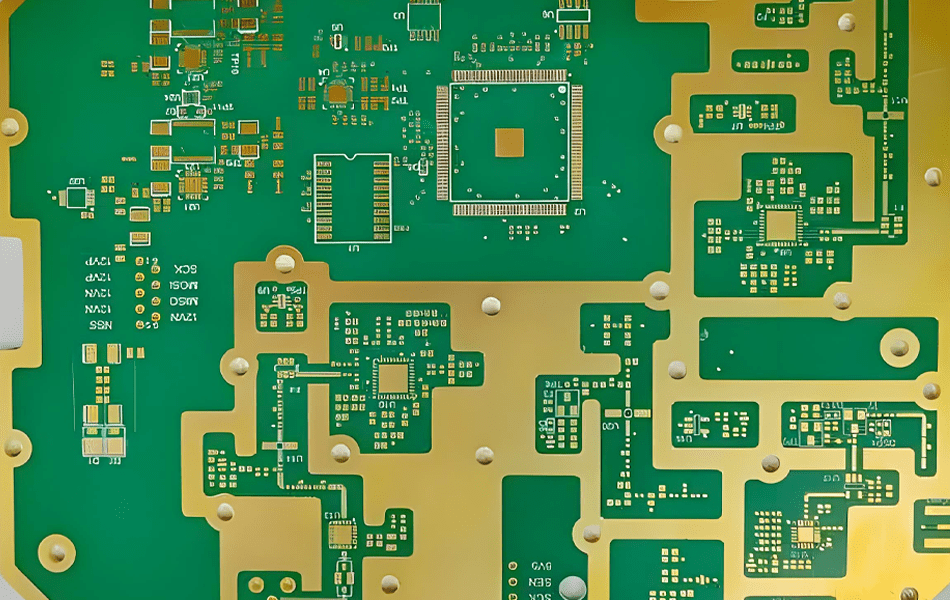
Where the Current Actually Flows
Conduction at high frequency is confined to a thin layer at the surface of the metal, and its thickness falls as the square root of frequency. The finish is applied at the surface, which is precisely where the current is, and the finish is not always a better conductor than the copper it covers.
| Metal | Skin depth at 1 GHz | 10 GHz | 77 GHz | Surface resistance at 10 GHz |
|---|---|---|---|---|
| Copper | 2.06 µm | 0.65 µm | 0.24 µm | 25.8 mΩ/sq |
| Silver | 2.01 µm | 0.64 µm | 0.23 µm | 25.1 mΩ/sq |
| Gold | 2.49 µm | 0.79 µm | 0.28 µm | 31.0 mΩ/sq |
| Nickel | 4.21 µm | 1.33 µm | 0.48 µm | 52.5 mΩ/sq |
| Palladium | 5.23 µm | 1.65 µm | 0.60 µm | 65.3 mΩ/sq |
| Tin | 5.26 µm | 1.66 µm | 0.60 µm | 65.6 mΩ/sq |
Two conclusions follow directly. Silver is essentially copper, so an immersion silver finish is electrically invisible. Nickel has 2.04 times the surface resistance of copper at every frequency, and the layers used in ENIG are several times thicker than the skin depth — so the current in an ENIG trace is nickel, not copper.
Why the Gold on ENIG Does Almost Nothing
Electroless nickel immersion gold deposits 3–6 µm of nickel and 0.05–0.1 µm of gold. At 10 GHz the skin depth in gold is 0.79 µm, so the gold layer is between one-sixteenth and one-eighth of a skin depth thick.
A layer thinner than the skin depth does not shield what is underneath it: the field penetrates through the gold and the current distribution is dominated by the nickel below. The gold exists to keep the nickel from oxidising and to present a solderable, wire-bondable surface. It is a chemical barrier, not a conductor, and the 0.1 µm of gold on a typical board carries a small fraction of the current.
This produces one of the more counter-intuitive results in high-frequency fabrication: adding gold to a nickel finish does not lower the loss, because the loss is set by the nickel underneath and the gold is too thin to matter.
What Nickel Costs in the Link Budget
How much the nickel costs depends on how much of the total loss was conductor loss to begin with, which is a property of the laminate.
- On FR-4, almost nothing. Dielectric loss dominates by an order of magnitude, so doubling the conductor term moves the total by a few per cent.
- On 5880 or TLY-5, a lot. With dielectric attenuation near 0.035 dB/in at 10 GHz and copper loss in the same range or higher, doubling the surface resistance can add 30–50% to total insertion loss.
- At 77 GHz, more. Skin depth in copper is 0.24 µm and the conductor term dominates the budget, so the finish choice becomes a first-order design decision rather than a procurement one.
The practical ranking for a low-loss build is OSP and immersion silver at the bottom of the loss table, ENIG and ENEPIG above them, and immersion tin worst — not because tin is a bad metal but because 1 µm of it at 10 GHz is most of a skin depth of a material with 2.5 times the resistivity of copper.
The Finish Options, and What Each Is For
| Finish | Thickness | RF cost | Chosen when |
|---|---|---|---|
| OSP | 0.2–0.5 µm organic | Lowest — no metal added | Short shelf life acceptable, single reflow, lowest loss wanted |
| Immersion silver | 0.1–0.3 µm | Very low — silver ≈ copper | Low loss plus solderability; needs sulphur-free packaging |
| ENIG | Ni 3–6 µm + Au 0.05–0.1 µm | Moderate — nickel at 2× Rs | Planarity, fine pitch, aluminium wire bonding |
| ENEPIG | Ni + Pd 0.05–0.15 µm + Au | Moderate to high — palladium at 2.5× Rs | Gold wire bonding, no black pad risk |
| Immersion tin | 0.8–1.2 µm | High | Press-fit and some press-fit connectors; whisker risk |
| Hard gold | 2–5 µm Au over Ni | Moderate | Edge connectors with wear; not a solderable finish |
OSP deserves a second look on high-frequency work because it adds no metal at all: the copper surface stays the conductor. Its limits are shelf life, the number of reflows it survives, and the fact that it is invisible — an OSP board that has been handled too much looks exactly like a good one until it is soldered.
Planarity, Solderability and the Trade Nobody Escapes
ENIG is popular on high-frequency boards for a reason that has nothing to do with loss: it is flat. Nickel builds a uniform layer over the copper, so fine-pitch pads and flip-chip sites stay coplanar, and that is worth more than a few tenths of a dB on many products.
The trade is explicit. OSP gives the best loss and the worst shelf life. Immersion silver gives nearly the best loss with good solderability, but the surface tarnishes and needs sulphur-free interleaving. ENIG gives planarity and a long shelf life at a measurable loss cost. ENEPIG adds a palladium layer that solves the black-pad mechanism and adds another resistive layer.
What cannot be done is to specify all four properties at once. That is why the finish belongs in the stack-up discussion next to the layer arrangement, not in a purchasing note written after the design is frozen.
The PTFE Interface
On fluoropolymer laminates the finish has a second job: it sits on copper that was plated onto a surface which had to be chemically modified to accept it. Residue from that modification — sodium naphthalene in particular — is a contamination source for the finish bath, and a poorly rinsed wall is where blistering starts.
Two practical consequences. Immersion silver on PTFE needs a clean, well-rinsed copper surface or the deposit is patchy. And any finish that requires a nickel strike or an activation step adds process steps over a surface that is already the weakest interface on the board — which is why the finish and the plating sequence are usually qualified together, as described in the plating guide.
The Field Failures Each Finish Carries
| Finish | Characteristic failure | Mechanism |
|---|---|---|
| ENIG | Black pad | Excess corrosion of the nickel during gold immersion; solder joint fails at the nickel |
| Immersion silver | Creep corrosion, tarnish | Sulphur and chlorine attack the silver along surfaces |
| OSP | Solderability loss after multiple reflows | Coating degrades; copper oxide forms under it |
| Immersion tin | Whiskers, tin pest | Stress-driven growth; low-temperature transformation |
| ENEPIG | Higher RF loss than expected | Palladium at 2.5× the surface resistance of copper |
Black pad is worth understanding because it is often blamed on the laminate. The mechanism is in the finish: if the nickel oxidises heavily before gold immersion, the gold deposit is porous and the nickel corrodes along the grain boundaries. It appears as a solder joint that wets, then fractures at the interface under thermal or mechanical load.
Where Surface Treatment Goes Wrong
| Symptom | Root cause in this step | Fix |
|---|---|---|
| Insertion loss 30–50% above simulation | ENIG nickel carrying the current on a low-loss laminate | Model the finish; consider OSP or immersion silver |
| Joints fracture at the pad interface | Black pad from heavy nickel oxidation | Nickel bath control; ENEPIG for critical joints |
| Tarnish and intermittent contact | Immersion silver exposed to sulphur | Sulphur-free packaging; controlled storage |
| Poor wetting on a second reflow | OSP consumed in the first pass | Match OSP grade to the reflow count |
| Patchy silver on PTFE | Na-naphthalene residue carried into the bath | Rinse verification; separate lines |
| Whiskers on fine pitch | Immersion tin stress | Avoid tin on fine pitch; anneal or change finish |
Surface Treatment Checklist
| # | Check | Pass condition |
|---|---|---|
| 1 | Finish chosen against the loss budget | Conductor term modelled with the finish resistivity |
| 2 | Nickel thickness justified | 3–6 µm; understood as 2× Rs at RF |
| 3 | Gold thickness stated | 0.05–0.1 µm and not counted as conductor |
| 4 | Reflow count matched to the finish | OSP grade or silver thickness specified |
| 5 | Shelf life and packaging | Sulphur-free for silver; sealed for OSP |
| 6 | Nickel bath control | Black-pad prevention, documented |
| 7 | PTFE rinse verified | No Na-naphthalene carry-over into the finish bath |
| 8 | Loss measured on the finished board | Not inferred from the laminate datasheet |
| 9 | Connector areas specified separately | Hard gold where wear, not solderability, is the requirement |
| 10 | Finish recorded per lot | Batch traceable to the bath |
Conclusion
Surface treatment is specified as a coating and behaves as a conductor. The organising fact is skin depth: at 10 GHz the current in copper lives in 0.65 µm, which is thinner than the nickel under an ENIG gold layer and much thinner than an immersion tin deposit. Whatever metal occupies that layer sets the conductor loss.
The claims worth discarding are that gold on ENIG improves RF performance (the gold is a fraction of a skin depth thick and the nickel underneath carries the current), that finish choice is a purchasing decision (on 5880 and TLY-5 it moves insertion loss by tens of per cent), and that any finish can be swapped without re-checking the loss budget.
XCE PCB applies OSP, immersion silver, ENIG, ENEPIG and hard gold on Rogers, Taconic and F4B builds, with the finish recorded per lot and loss measured on the finished article: 2–72 layers, impedance ±10%, panels to 600 × 1200 mm, 5,000 m² of production space and 80+ engineers, with samples in as fast as 24 hours.
The same finishes, compared on the terms a purchase order can enforce — IPC thickness windows, phosphorus content, shelf life, cost per square foot and the one failure mode each carries — are set out in PCB surface treatment processes, which covers all eight finishes rather than the five that appear on RF laminates.
Frequently Asked Questions
Does ENIG affect high-frequency performance?
Which finish has the lowest loss?
What is skin depth at 10 GHz?
Why use ENIG on a high-frequency board at all?
What causes black pad?
Can I change finish without re-checking the design?
Need a Finish That Suits the Loss Budget?
Send us your Gerber files and requirements for a manufacturability review and a tailored quotation.
sales1@xcepcb.com
+86 180 3341 4657