
An RF PCB is any board whose traces are large enough, relative to the signal’s wavelength, that the trace stops behaving like a wire and starts behaving like a transmission line. That single definition drives everything else: the materials, the impedance tolerance, the finish and the test plan. This article sets out the performance characteristics that define an RF board, then walks through the industries it serves — correcting along the way several applications that are routinely but wrongly attributed to RF boards.
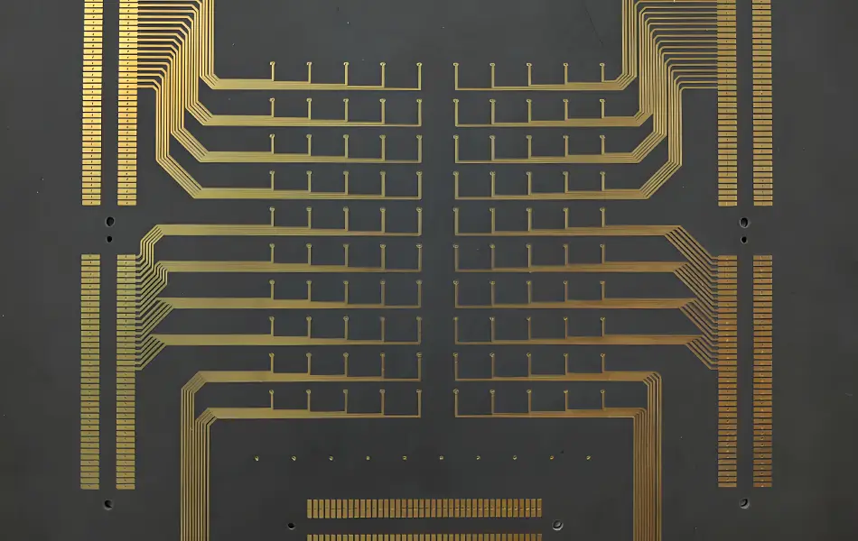
What Makes a Board an RF Board
The dividing line is physical, not a marketing tier. When the signal wavelength becomes comparable to the trace dimensions — conventionally somewhere above a few hundred megahertz, and certainly by the low gigahertz — reflections, losses and radiation dominate ordinary circuit behaviour. From that point the board is a set of transmission lines, and three things change:
- The laminate stops being commodity. Standard FR-4 loses 1.08 dB/in at 10 GHz — thirty times a purpose-built RF laminate — and its Dk wanders with frequency and resin content.
- Impedance becomes a specification. Digital boards tolerate impedance spread; RF boards buy it: 50 Ω ±10%, verified by coupon TDR in the product’s own lamination cycle.
- Surface details become electrical. The finish, the mask and the copper roughness all sit inside the skin depth — 0.65 µm at 10 GHz — and each one measurably changes loss.
Note what this excludes: a Wi-Fi module on a thick FR-4 board with no controlled impedance is not an RF board just because it handles 2.4 GHz, and a 10 GHz equalised digital link is not an RF board just because it is fast. The definition is about controlled transmission-line behaviour, as the RF PCB primer lays out.
The Four Properties That Define RF Performance
| Property | What it sets | Working numbers |
|---|---|---|
| Dielectric constant (Dk) | Signal speed and trace width; a stable, frequency-flat Dk makes phase predictable | 2.20 (5880) to 10.2 (RO3010); process vs design Dk must not be mixed up — RO3010 is 10.2 processed, 11.20 in design tables |
| Dissipation factor (Df) | Dielectric loss — the dominant loss term at microwave frequencies | 10 GHz attenuation ≈ 2.6 × f × √Dk × Df dB/in: FR-4 1.08, RO4350B 0.18, 5880 0.035 |
| Thermal behaviour | Survival at reflow and over cycles; phase drift in service | Z-CTE vs copper 17 decides barrel reliability; TCDk sets phase drift (~11° per 100 mm line across −50…+150 °C at +50 ppm) |
| Mechanical and finish properties | Manufacturability and the conductor itself | PTFE is soft and creeps (finish machining sets final size); the finish sits in the skin depth, so ENIG nickel can add 30–50% loss on low-Df laminates |
Signal integrity is not a fifth property — it is the consequence of holding the four above across the whole board: continuous reference planes, impedance windows kept, transitions minimised. The design-steps guide covers the layout side.
Thermal Performance: the Honest Version
RF laminate marketing often lists “high thermal conductivity” as a property. For the standard RF materials it is not: PTFE laminates run 0.20–0.33 W/m·K and hydrocarbon ceramics 0.66–0.95 — all of them insulators compared with copper’s 400. A 0.254 mm layer of RO4350B has the same thermal resistance as 142 mm of copper.
What RF boards actually do about heat:
- Thermal vias carry the vertical path from hot components to internal planes or a back-side heatsink — arrays of 0.3–0.5 mm holes at 0.8–1.0 mm pitch.
- Copper pours spread laterally, but only on layers, not through the dielectric.
- Material choice manages the failures heat causes, not the heat itself: Z-CTE keeps barrels intact through reflow and cycling, and Td (390–500 °C across the common laminates) keeps the material intact through assembly.
The distinction matters at procurement: a laminate chosen for “thermal conductivity” it does not have, at the expense of the electrical properties it does, is a mis-specified board.
Where RF PCBs Actually Go
| Sector | Real RF role | Typical requirements |
|---|---|---|
| Wireless infrastructure | Base-station PAs, filters, antenna feed networks, AAU front ends | Low Df, TCDk-matched stacks, high power handling, 102-inch antenna-class low PIM on Taconic RF-30 |
| Satellite and aerospace | Transponders, phased arrays, TT&C links | Outgassing (NASA TML/CVCM), Z-CTE discipline on multilayer PTFE, low loss at Ku/Ka band |
| Defence radar and EW | Phased-array panels, receivers, jammers, guidance links | Phase stability over temperature, stripline isolation, ITAR-class traceability |
| Automotive | 24/77 GHz radar boards, V2X and telematics radios | RO4000-class laminates (4350B/4835), AEC-Q-aligned reliability, TCDk for beam-forming |
| Medical | MRI RF coils, microwave ablation, wireless telemetry, patient monitors’ radio links | Ultrasound and MRI front ends are genuinely RF; biocompatibility belongs to the finished device (ISO 10993), not the laminate |
| Consumer and wearables | Phone/Wearable RF front-end modules, antenna-in-package, UWB and GNSS sections | Miniaturised high-Dk materials (RO3010-class) to shrink antennas, low cost at volume |
Applications Commonly Claimed That Are Not RF
The application lists circulating on RF PCB pages usually overreach, and the overreach is diagnosable. Four examples worth naming, because buyers repeat them:
| Claimed | Reality |
|---|---|
| CT imaging | Computed tomography is X-ray based — no RF signal in the imaging chain. The RF PCB list at a hospital belongs to MRI coils and telemetry, not CT. |
| Blood-glucose and heart-rate monitors as RF devices | The sensing electronics are analogue and low frequency. The RF board’s role, where present, is the Bluetooth/NB-IoT link that reports the reading — a module, not the monitor. |
| Camera systems “processing high-frequency signals” | Imaging pipelines are digital and high-speed — a different discipline. The RF content of a camera product is its wireless interface. |
| Smartphone wireless charging | Charging coils are power electronics at kilohertz frequencies. The RF PCB in a phone is the front-end module: PA, filters, switches, antennas. |
The honest framing is not smaller — it is more specific. RF boards carry the radio. Everything else on the product is another board’s problem, and pretending otherwise mis-specifies both.
How RF Requirements Change Fabrication
The same factory makes both board types, but RF builds change the recipe at five points:
- Material handling. PTFE laminates need plasma or sodium-naphthalene hole treatment, FEP-family bonding films pressed at 260–300 °C, and dry drilling — standard FR-4 desmear chemistry does nothing to PTFE.
- Impedance process control. Etch compensation by copper weight, 0.5 oz copper under 0.15 mm lines, pressed-height specification instead of nominal, coupon TDR per batch — the closed loop in the impedance-control guide.
- Finish selection by loss budget. Where the link budget is tight, OSP or immersion silver; ENIG where fine pitch and shelf life win. The trade is quantified in the surface-treatment guide.
- Hybrid stack discipline. RF layers outside, FR-4 core centred, bonding materials compatible with both chemistries, hole files split by span.
- Test plan with electrical teeth. AOI and flying probe still run, but the batch ships or stops on coupon impedance data and, where specified, VNA loss.
What to Ask an RF PCB Supplier
- Which laminates are stocked and qualified — genuine Rogers/Taconic/F4B stocking, with data sheets traceable to the material lot, not “equivalent” claims.
- How impedance is verified — coupon in the product lamination cycle, five per batch, Cpk reported; not a one-time golden-board measurement.
- PTFE process capability — plasma/sodium-naphthalene line, FEP bonding capability, dry routing, and the aspect-ratio limit they will actually commit to (6:1 is a fair bar).
- What the report contains — coupon TDR values, loss data where asked, finish and thickness records, material certificates.
- Speed and scale — sample lead time for RF builds and monthly capacity, because a qualified process that cannot scale is a pilot line.
XCE PCB answers those questions with numbers: 2–72 layers, impedance ±10%, panels to 600 × 1200 mm, 5,000 m² of production space and 80+ engineers, samples in as fast as 24 hours.
Conclusion
RF PCB performance is a short list of properties — dielectric, thermal, mechanical, finish — held to tolerances that ordinary boards never face, and RF functions are similarly specific: the board carries the radio, from base-station PAs to radar arrays to the front-end module in a wearable. The industry lists that pad RF applications with CT scanners and glucose monitors do the opposite of selling: they blur exactly the boundary a buyer is paying a specialist to respect.
XCE PCB fabricates RF boards on Rogers, Taconic and F4B laminates with coupon-verified impedance and finish-appropriate processing: 2–72 layers, impedance ±10%, panels to 600 × 1200 mm, 5,000 m² of production space and 80+ engineers, with samples in as fast as 24 hours.
Frequently Asked Questions
At what frequency does a PCB become an RF PCB?
Do RF laminates have high thermal conductivity?
Are CT scanners, glucose monitors and cameras RF applications?
What makes automotive radar an RF PCB job while ADAS cameras are not?
Why does the surface finish appear in RF performance discussions?
What should I verify before choosing an RF PCB manufacturer?
Building an RF Board? Talk to a Specialist
Send us your Gerber files and requirements for a manufacturability review and a tailored quotation.
sales1@xcepcb.com
+86 180 3818 8537