
Copper thickness is specified in ounces, drawn in microns, measured in mils and inspected on a cross-section — four units for one dimension, which is where most of the confusion starts. The second source of confusion is attribution: thickness is credited with improving impedance, delay, inductance and corrosion resistance, none of which it does. This article gives the conversion table, the current and loss numbers, and an honest list of what copper weight actually buys.
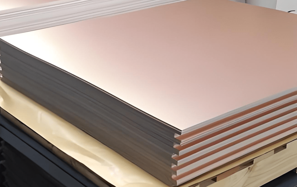
Two Thicknesses Share One Name
“1 oz copper” on an outer layer and “1 oz copper” on an inner layer are not the same finished dimension. The ounce figure describes the base foil: 1 oz of copper spread over one square foot is 35 µm thick. What ends up on the board depends on what happens afterwards.
| Where | What “1 oz” finishes at | Why |
|---|---|---|
| Inner layer | About 35 µm (foil, untouched) | Inner layers are etched from base foil; plating only adds inside drilled holes |
| Outer layer, pattern plated | About 50–60 µm (35 + 20–25) | The same plating step that metallises the barrels adds copper to the surface |
| Outer layer, panel plated then etched | About 35 µm nominal, minus etch | Plated everywhere, then the surface is etched back to the pattern |
| Via barrel | 20–25 µm wall | Plating thickness in the hole, not on the surface |
The practical consequence: a callout of “1 oz finished” on an outer layer is a different requirement from “1 oz base”, and a quotation based on the wrong one is either 40% light or 40% expensive. State which you mean, and if the design is impedance-controlled, state the thickness the field solver used — because that is the number the geometry was calculated from.
The Conversion and Current Table
Resistance figures are for a 1 mm wide trace at 20 °C, using copper resistivity of 1.68 × 10⁻⁸ Ω·m. Current figures are order-of-magnitude for a 10 °C rise on an external layer in still air; treat them as a starting point for a real thermal calculation, not as a rating.
| Copper weight | Thickness | Sheet resistance | 1 mm wide, 1 m long | Current, 1 mm, 10 °C rise (external) |
|---|---|---|---|---|
| 0.25 oz | 8.75 µm | 1.92 mΩ/sq | 1.92 Ω | ~0.9 A |
| 0.33 oz | 12 µm | 1.40 mΩ/sq | 1.40 Ω | ~1.0 A |
| 0.5 oz | 17.5 µm | 0.96 mΩ/sq | 0.96 Ω | ~1.4 A |
| 1 oz | 35 µm | 0.48 mΩ/sq | 0.48 Ω | ~2.3 A |
| 2 oz | 70 µm | 0.24 mΩ/sq | 0.24 Ω | ~4.0 A |
| 3 oz | 105 µm | 0.16 mΩ/sq | 0.16 Ω | ~5.3 A |
| 4 oz | 140 µm | 0.12 mΩ/sq | 0.12 Ω | ~6.5 A |
| 6 oz | 210 µm | 0.08 mΩ/sq | 0.08 Ω | ~8.8 A |
Two readings matter. Current does not scale linearly with thickness, because a wider or thicker trace also has more surface from which to convect — and, more importantly, because the surrounding board conducts heat away. The old IPC-2221 charts remain in common use; IPC-2152 superseded them with a more realistic treatment of the thermal environment, and its results are frequently lower for the same geometry. On internal layers, expect roughly half the external current for the same rise.
The second reading is that resistance is the honest currency here, not ounces. A 0.5 mm wide 1 oz trace has the same resistance as a 0.25 mm wide 2 oz trace — one costs routing area, the other costs copper and etch capability.
What Thickness Actually Buys
- DC resistance and IR drop. Linear in thickness. This is the primary and least arguable benefit.
- Current-carrying capacity. Follows resistance, with the thermal caveat above.
- Lateral heat spreading. Thick copper spreads heat across the board surface, which lowers hot-spot temperature under a dissipating part. This is a real thermal function, distinct from the vertical path through the dielectric.
- Conductor loss at high frequency, but only up to a point. Once the copper is several skin depths thick, adding more does nothing for loss. At 10 GHz the skin depth in copper is 0.65 µm, so 0.5 oz is already 27 skin depths. That is why RF boards use thin, smooth foil and heavy copper buys nothing there.
- Mechanical robustness at connectors and edges. Heavy copper resists pad lift and edge damage at card-edge fingers and press-fit holes.
- Etch capability — in the negative direction. Thicker copper loses more width to side etch and therefore cannot hold fine lines. This is the constraint that usually decides the choice, and it is covered next.
Thick Copper and Fine Lines Are Opposed
Wet etching removes copper sideways at a rate proportional to how long it takes to go through the thickness, so side etch per edge is roughly copper thickness divided by the etch factor (about 2.5 for spray etching). The result is a hard floor on achievable line width for each copper weight:
| Copper weight | Side etch per edge (EF 2.5) | Practical minimum line | Consequence |
|---|---|---|---|
| 0.5 oz (17.5 µm) | 7 µm | ~0.075 mm | The fine-line choice: RF, HDI, dense digital |
| 1 oz (35 µm) | 14 µm | ~0.10 mm | The default for general boards |
| 2 oz (70 µm) | 28 µm | ~0.15 mm | Power layers; fine-pitch escape becomes impossible |
| 4 oz (140 µm) | 56 µm | ~0.25 mm | Heavy copper: motor drives, high-current bus bars |
A 0.10 mm line in 2 oz foil loses 28 % of its width to side etch per edge, which is both a resistance problem and a mechanical one. This is why heavy-copper designs and fine-pitch designs are almost never the same board, and why “use 2 oz everywhere for current” fails on any board with a 0.4 mm pitch package on it. The usual resolution is a mixed stack: heavy copper on the power layers, 0.5–1 oz on the signal layers.
What Thickness Does Not Change
| Property | Effect of copper thickness | What actually governs it |
|---|---|---|
| Characteristic impedance | Small — roughly 1–4% per doubling of weight on a thin dielectric, as a second-order term next to height | Dielectric height and Dk. Thickness changes the drawn width needed for 50 Ω, not the physics |
| Propagation delay | Effectively none | Delay is length × √εeff / c. Copper thickness does not enter |
| Inductance | Minor | Loop geometry: trace width, height above the reference plane, return path proximity |
| Corrosion resistance | Delays, does not prevent | Surface finish: ENIG, immersion silver, OSP. Thick bare copper oxidises just as readily |
| Board stiffness | A few percent; can worsen warp if unbalanced | Substrate modulus and thickness. Copper is 35 µm against a 1.6 mm board |
| Signal integrity at high frequency | None once thickness exceeds a few skin depths | Foil roughness, finish, dielectric loss |
The impedance row deserves a practical note: because thicker copper widens the effective conductor, a design recalculated from 0.5 oz to 1 oz usually needs a slightly narrower trace to stay at 50 Ω — on the order of 2–3% per doubling of weight. If the width is not recalculated, the board comes back a couple of ohms low, which is inside a ±10% window and outside a ±5% one.
Heavy Copper Is a Different Process
Above 3 oz, and certainly at 6 oz and beyond, the constraints stop being electrical and become manufacturing:
- Etching needs specialised lines — thicker resist, tighter rate control, sometimes etching from both sides in stages, because a 210 µm layer does not clear uniformly.
- Lamination is harder: thick copper topography means the prepreg has to fill deeper valleys, and resin-starved areas become void sites.
- Drilling removes more copper per hit, so bit wear and entry/exit quality change; burr control becomes a specification rather than a housekeeping matter.
- Solder mask must be applied thicker to cover the step at trace edges, or it will thin over the copper and fail adhesion.
- Minimum line width and spacing grow together, which is why heavy-copper boards look sparse.
None of this is exotic — it is routine for motor drives, power supplies and automotive bus bars — but it is a different quote from a 1 oz digital board, and it needs to be flagged before layout rather than after.
Specifying and Inspecting It
- Say base or finished, per layer, and give the tolerance: typically nominal ±10%, with a minimum that matters more than the nominal for current.
- Give the current and the allowed rise rather than a weight, when current is the reason. A fabricator can meet 3 A at 15 °C with more than one combination of weight and width.
- Name the impedance-relevant thickness for controlled-impedance layers, because it is the field solver’s input.
- Inspect on a cross-section, at the coupon and at a representative trace, and record both surface and barrel copper. Surface-only measurement is the classic way to accept a board whose barrels are thin.
- For RF layers, pair the thickness callout with a foil type — roughness matters more than microns, as the high-frequency copper thickness article sets out.
Claims That Do Not Hold
| Claim | Reality |
|---|---|
| “Thick copper reduces inductance and therefore improves signal integrity” | Inductance is set by loop geometry. Thickness changes it marginally; the return path is worth an order of magnitude more |
| “Thick copper reduces signal delay” | Delay depends on Dk and length. Copper thickness is not a term in the equation |
| “Thick copper resists corrosion better in harsh environments” | It delays consumption of the copper, but the corrosion rate is set by the surface finish and the environment. Bare heavy copper oxidises exactly like bare thin copper |
| “Thick copper lets you use fewer layers” | Only for current-carrying nets, where one heavy layer can replace several paralleled thin ones. It does nothing for signal layer count and it blocks fine-pitch routing |
| “Thick copper makes the board stiffer” | Marginally, and asymmetrically: copper on one side only increases warp. Stiffness comes from the substrate |
| “More copper always means lower loss” | Only below a few skin depths. At 10 GHz the current lives in 0.65 µm; 0.5 oz is already 27 times that |
Conclusion
Copper thickness is a DC and thermal decision first, an etch-capability constraint second, and an RF decision almost never. Get the unit right — base or finished, per layer — then use resistance rather than ounces as the currency, and check that the fine-pitch packages on the same board can survive the weight the power nets want. Everything else credited to copper thickness is either a second-order effect or belongs to the finish, the dielectric or the return path.
Two adjacent decisions interact with this one: how the thickness is pressed and bonded is the lamination subject, and how the etched width is controlled is the impedance subject. The vocabulary for both — base foil, panel plating, pattern plating, side etch — is in the PCB processing terminology article.
XCE PCB processes 0.25–6 oz copper with heavy-copper etching and cross-section verification: 2–72 layers, impedance held to ±10%, panels to 600 × 1200 mm, 5,000 m² of production space and 80+ engineers, with samples in as fast as 24 hours.
Frequently Asked Questions
What does 1 oz copper mean in microns?
How much current can 1 oz copper carry?
Does copper thickness affect impedance?
Why can’t I use 2 oz copper with fine-pitch components?
Does thicker copper reduce high-frequency loss?
How is copper thickness verified?
Heavy Copper or Fine Lines? Send Us the Stack
Send us your Gerber files and requirements for a manufacturability review and a tailored quotation.
sales1@xcepcb.com
+86 180 3341 4657