
Every step before lamination is a promise about dielectric height. The stack-up assumes it, the etch sizes the trace to it, the impedance model is solved against it — and none of them can measure it. The press turns that assumption into a physical number, which is why lamination, not routing or test, is where a high-frequency impedance spec is finally decided. It is also the step most often described in vague terms, because the interesting part is a set of temperatures, pressures and flow numbers that differ completely between FR-4, RO4000 laminate and PTFE.
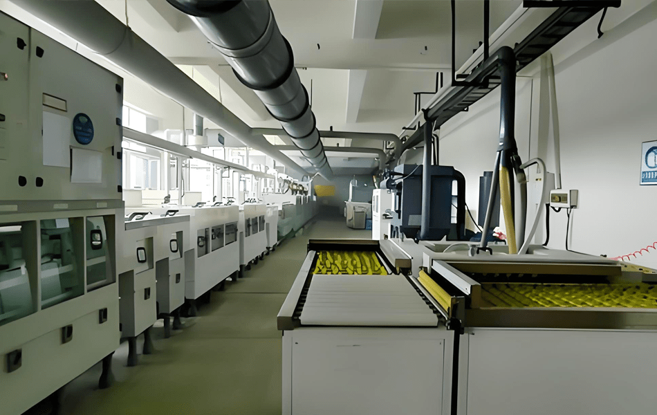
Why the Press, and Not the Design, Decides Impedance
Impedance on a microstrip is a function of three numbers: trace width, dielectric height and dielectric constant. All three are chosen in the design; only one of them is physically produced by the etcher, and only two of them are physically produced here. Width is set by the previous step, described in the inner-layer fabrication guide. Height and Dk come out of the press.
That is the whole reason lamination deserves its own process window rather than a line in a router program. A stack-up that says “0.254 mm RO4350B” is describing a core, not the dielectric the field sees. The field sees the core plus the bond ply after the resin has flowed, and the difference between a bond ply that presses to 0.10 mm and one that presses to 0.08 mm is a 5.6% change in height and about 3% in impedance — larger than the entire Dk tolerance of the laminate.
This is step five in the twelve-step manufacturing sequence, immediately after the cut, pinned and imaged inner layers covered in the substrate cutting guide. Everything after it — drilling, plating, finish — can only preserve what the press produced.
Role 1 — The Dielectric Height Is Made Here, Not Specified on a Datasheet
Laminate datasheets quote a nominal thickness with a tolerance of about ±10% on unfilled PTFE and tighter on ceramic-filled grades. That tolerance is not a manufacturing detail; it is the dominant term in the impedance budget, and it lands entirely on this step.
| Pressed height on a 0.254 mm nominal build | Height error | Impedance of a 0.56 mm line (Dk 3.66) | Impedance error |
|---|---|---|---|
| 0.2286 mm | −10% | 46.8 Ω | −6.5% |
| 0.2413 mm | −5% | 48.4 Ω | −3.2% |
| 0.2540 mm | nominal | 50.0 Ω | — |
| 0.2667 mm | +5% | 51.6 Ω | +3.1% |
| 0.2794 mm | +10% | 53.0 Ω | +6.1% |
Two conclusions follow. First, a ±10% height tolerance alone consumes ±6% of a ±10% impedance specification, which leaves very little room for width error, Dk error and copper thickness error to be added on top — the budget that the design step guide sets out in full. Second, the only useful height number is the one measured on the pressed panel, not the one ordered from the laminate supplier.
The practical consequence is that the press is run to a target pressed thickness, with coupons on the panel and a first-article section, rather than to a recipe that worked last month on a different lot of core.
Role 2 — The Bond Ply Is a Third Dielectric, and It Flows
The layer that joins two cores is not a glue line. On an RO4000 build it is a prepreg such as 4450B with a dielectric constant close to the core; on a PTFE build it is a FEP bonding film with a dielectric constant near 2.1, which is well below the laminate it joins. Either way it is electrically in series with the core, and its final thickness is a process output, not a purchased dimension.
Resin flow, typically 15–25% of the prepreg’s resin content under a normal cycle, is what sets that final thickness. Two failure directions:
- Too little flow. The bond ply stays thick, the gap grows, and impedance reads high. A bond ply that presses to 0.12 mm instead of 0.10 mm on a 0.254 mm core puts the total gap 5.6% over nominal, which is 3% on impedance and is usually blamed on the laminate.
- Too much flow. Resin leaves the bond line, the gap closes, and impedance reads low. Worse, resin starvation leaves dry glass at the edge of large copper features, which is where delamination starts after thermal cycling.
On PTFE the arithmetic is different because the bonding film is not a filled prepreg: a FEP layer 0.05 mm thick, with a Dk of roughly 2.1 against 2.2 for the laminate, is nearly matched and mostly acts as extra height. On a ceramic-filled build, by contrast, a 3.5-Dk bond ply between 3.0-Dk cores lowers the effective Dk of the gap slightly while adding height — two effects that partly cancel, which is why the stack-up has to be solved with the bond ply included rather than added afterwards. The hybrid design file guide covers what happens when it is left out.
Role 3 — Registration: The Panel Shrinks, the Fiducials Do Not
Prepreg cures by cross-linking, and cross-linking shrinks. The number is small — 0.02% to 0.05% linear in the plane — and the panel is large, so the product is not small at all.
| Cure shrinkage | Movement across a 600 mm panel | Against a ±0.05–0.075 mm registration budget |
|---|---|---|
| 0.02% | 0.12 mm | 1.6–2.4× the budget |
| 0.03% | 0.18 mm | 2.4–3.6× the budget |
| 0.05% | 0.30 mm | 4–6× the budget |
The movement is also anisotropic: glass styles shrink more along the weft than the warp, so a single scale factor applied to both axes over-corrects one of them. The workable approach is to press a scale-factor panel from the same lot of prepreg, measure the movement in X and Y separately, and apply both factors to the drill program — which is why the drill file has to be released after lamination, not before.
For high layer counts this is the same budget described in the inner-layer article: a ±0.075 mm layer-to-layer error already consumes a 0.05 mm annular ring, and a 0.18 mm panel shrink applied on top of it turns every via into a breakout unless it is compensated.
Role 4 — Thermal: What the Press Does, and What a “Heat Spreading Layer” Cannot Do
The usual claim is that lamination aids thermal management by distributing conductive or heat-dissipating layers through the stack. The first half is true and the second half is a category error, so it is worth putting a number on the vertical path.
Thermal resistance per unit area is thickness divided by conductivity. For 0.254 mm of RO4350B at 0.69 W/m·K that is 3.7×10⁻⁴ m²K/W — the same resistance as 142 mm of copper. For the same thickness of FR-4 at 0.3 W/m·K it is equivalent to 326 mm of copper.
| Dielectric, 0.254 mm | k (W/m·K) | Equivalent copper thickness | Rise at 10 W/cm² |
|---|---|---|---|
| FR-4 | 0.30 | 326 mm | 85 K |
| RO3003 | 0.50 | 196 mm | 51 K |
| RO4350B | 0.69 | 142 mm | 37 K |
| RO3010 | 0.95 | 103 mm | 27 K |
Read the last column and the design rule is obvious: the dielectric, not the copper planes, is the barrier, and putting an extra copper layer in the middle of the stack does not shorten the path through it. What actually lowers the through-thickness resistance is copper that crosses the dielectric — thermal vias, filled and capped, under the dissipating component. High-frequency laminate helps because 0.69 versus 0.30 W/m·K is a real 2.3×, but the press does not add thermal performance; it only has to avoid trapping voids, which are far better insulators than the resin around them.
The Press Cycle, Material by Material
There is no universal lamination profile, and the reason is that the three material families bond by three different mechanisms. FR-4 prepreg cures; RO4000 prepreg cures at a higher temperature with a different resin chemistry; PTFE does not cure at all and has to be welded with a fluoropolymer film that melts.
| Build | Bond medium | Hold temperature | Pressure | Dominant failure |
|---|---|---|---|---|
| FR-4 multilayer | FR-4 prepreg | 170–190 °C, 60–90 min | 200–400 psi | Resin starvation, pink ring |
| RO4000 (4350B / 4003C) | 4450B prepreg | 190–200 °C, 60–90 min | 200–400 psi | Height drift from flow; low flow at the edges |
| Ceramic PTFE (3003 / 3010) | FEP bonding film | 260–300 °C | 150–300 psi | Bond film squeeze-out, voids over large copper |
| Pure PTFE (5880 / TLY-5) | FEP bonding film | 260–300 °C | 150–250 psi | Cold flow — the dielectric thins under load |
| PTFE + FR-4 hybrid | Two-stage, or a low-temperature bond film | Cannot be co-cured in one cycle | — | FR-4 degradation if pressed at PTFE temperature |
The last row is the one that catches projects. FR-4 cures at 170–190 °C and begins to degrade well before the 260–300 °C a fluoropolymer bond needs, so a PTFE/FR-4 hybrid cannot be built in a single press cycle: the PTFE sub-assembly is bonded first, then the FR-4 portion is laminated onto it with a bond film that cures below the PTFE joint’s service limit. The process detail is set out in the 5880 and FR-4 lamination guide and in the hybrid lamination analysis.
Ramp rate matters as much as hold temperature: 2–3 °C per minute through the resin’s softening range lets volatiles escape and lets the resin reach the same viscosity everywhere on the panel. A fast ramp cures the outside of the panel while the centre is still cold, and the resulting height gradient across a 600 × 1200 mm press opening is one of the quieter causes of impedance spread.
Pressure Is a Thickness Control, Not a Force Setting
Pressure is usually written as a number and treated as a constant. It is the second knob on pressed height, and it behaves differently on each material family.
- Too much pressure on a thermoset build. Resin is squeezed out of the bond line: the gap closes, Dk rises slightly as the filler fraction goes up, and the panel reads low in impedance with a dry, glossy edge as the visible symptom.
- Too little pressure. Air is not expelled, the gap stays thick, and the panel reads high — while the voids left behind lower Dk locally, which is a second and larger error in the same direction as the first.
- PTFE is different: it cold-flows. A fluoropolymer has no cross-linked network to resist deformation, so pressure that would be normal on FR-4 permanently thins the dielectric. A 4% loss of height on a 0.254 mm build moves a 50 Ω line to 48.8 Ω, and the loss does not recover when pressure is released.
That last point is why PTFE builds are specified with a thicker starting laminate and pressed at 150–250 psi rather than at the 300–400 psi a thermoset would take, and why the pressed thickness of every PTFE panel should be measured rather than assumed to equal the core plus the film.
Voids: a 10 µm Air Layer Is a 9.5% Dk Error
A void is not just a cosmetic defect and a delamination seed. Air has a dielectric constant of 1.0 against 3.66 for RO4350B, so any air trapped in the gap is in series with the dielectric and pulls the effective Dk down — sharply, because the contrast is large.
| Air layer inside a 0.254 mm gap | Effective Dk | Dk error | Impedance of the 0.56 mm line |
|---|---|---|---|
| 5 µm | 3.48 | −5.0% | 51.2 Ω (+2.3%) |
| 10 µm | 3.31 | −9.5% | 52.3 Ω (+4.6%) |
| 20 µm | 3.03 | −17.3% | 54.4 Ω (+8.8%) |
| 50 µm | 2.40 | −34.4% | 60.1 Ω (+20.2%) |
A 10 µm air layer is thinner than a human hair and is invisible to a thickness gauge, yet it costs half the impedance budget. And because voids are local, a panel can average exactly 50 Ω on its coupon while individual traces over a large ground pour read 52 Ω — a step in the TDR trace that no average will reveal.
Where voids come from is worth listing, because all of it is preventable in this step: air left under a large copper area with no vent path, moisture in the prepreg (hence the 120–150 °C bake for FR-4 cores before pressing), contamination or burrs on the inner layer, insufficient vacuum, and too-fast a ramp trapping volatiles before the resin can flow.
Cooling, Residual Stress and the Height That Comes Back
Cooling is not a passive wait. It is where the residual stress field of the finished board is set, and on PTFE it is also where the dielectric height changes by a measurable amount.
The rule is to hold pressure until the panel is below the resin’s glass transition, then cool at 2–3 °C per minute. Releasing pressure while the stack is still hot lets the layers shear against each other; cooling faster than that locks in a gradient between the surface and the core, which shows up as bow and twist after routing.
The PTFE number is the one most often missed. Z-axis CTE for RT/duroid 5880 is 237 ppm/°C and for TLY-5 is 217, against 25 for RO3003 and 16 for RO3010. Over a 20 °C to 150 °C excursion, a 0.254 mm build of 5880 grows 7.8 µm in thickness — 3.08% — and the impedance rises about 1.9% with it, on top of whatever the Dk does with temperature.
| Laminate | Z-CTE (ppm/°C) | Height change, 20→150 °C on 0.254 mm | Effect on impedance |
|---|---|---|---|
| RT/duroid 5880 | 237 | +7.8 µm (+3.08%) | +1.9% |
| Taconic TLY-5 | 217 | +7.2 µm (+2.82%) | +1.7% |
| RO4350B | 32 | +1.1 µm (+0.42%) | +0.3% |
| RO3003 | 25 | +0.8 µm (+0.33%) | +0.2% |
| RO3010 | 16 | +0.5 µm (+0.21%) | +0.1% |
This is a materials distinction, not a process one: the ceramic-filled grades hold their height with temperature because the ceramic filler has a low expansion coefficient, while unfilled PTFE expands ten times more. On a phase-critical design in 5880 the thickness term is of the same order as the Dk term, and both are usually attributed to “the material” without separating them.
Offset Stripline: Asymmetry Costs More Than Thickness
In stripline the trace sits between two reference planes, so the relevant height is the sum of both dielectric gaps — and that sum is built from two separately pressed bond lines. If one side flows more than the other, the trace is no longer centred, which changes impedance even when the total is correct.
Take a 50 Ω stripline sized for a 0.5 mm total gap (0.222 mm trace on Dk 3.66). Press the stack so the total gap moves by 10% and impedance follows the gap directly:
| Pressed total gap | Change | Impedance |
|---|---|---|
| 0.45 mm | −10% | 46.4 Ω (−7.2%) |
| 0.50 mm | nominal | 50.0 Ω |
| 0.55 mm | +10% | 53.2 Ω (+6.4%) |
Stripline is more sensitive than microstrip to the same percentage change, because both halves of the gap contribute and because the field is fully enclosed. It is also the geometry that fails latest in the process: microstrip impedance can be checked on the outer layer after finish, while a buried stripline can only be measured by TDR on a coupon or by cross-section — so the press is the last opportunity to get it right, as laid out in the stack-up design guide.
What Inspection Can and Cannot See After the Press
Four checks belong to this step, and each answers a different question.
| Check | What it proves | What it misses |
|---|---|---|
| Ultrasonic C-scan | Delamination and large voids between layers | Voids below roughly 1 mm lateral; anything inside a core |
| Cross-section | Bond line thickness, resin squeeze, plated hole shape | Only the plane it cuts; no statistics |
| Thickness measurement | Pressed height at the coupon and at the panel edge | Any local variation between the two points |
| TDR on coupon | The impedance the process actually produced | Per-trace variation on the product itself |
Between them these cover delamination, height and impedance. None of them measures the Dk of the pressed dielectric, the filler distribution across the panel, or the foil profile that sets conductor loss — so a panel can pass every check and still miss a loss target. That is not a reason to add inspections; it is a reason to keep the press cycle recorded per lot, so that when a lot does come back wrong the cycle can be compared rather than guessed at.
Where Lamination Goes Wrong
| Symptom | Root cause in this step | Corrective action |
|---|---|---|
| Impedance 3–6% high across a lot | Bond ply under-flowed, or the stack-up height was quoted as bare core | Press to measured thickness; count the bond ply in the stack-up |
| Impedance low with a dry panel edge | Excess pressure squeezing resin out of the bond line | Reduce pressure 50 psi; check prepreg flow against its datasheet |
| Voids over large copper, coupon still in spec | No vent path, moisture, or too fast a ramp | Vent the copper, bake the cores, 2–3 °C/min ramp |
| Vias breaking out on one edge only | Prepreg cure shrink not compensated per axis | Press a scale panel, apply X and Y factors separately |
| Delamination after thermal cycling | Oxide dissolved by moist prepreg, or resist residue at the interface | Bake, thin oxide or oxide alternative, water-break test |
| PTFE panel thinner than ordered | Cold flow under a pressure meant for thermoset | 150–250 psi, thicker starting laminate, measure every panel |
| Bow and twist after routing | Pressure released hot, or asymmetric copper distribution | Hold pressure below Tg, balance copper, cool 2–3 °C/min |
Lamination Checklist
| # | Check | Pass condition |
|---|---|---|
| 1 | Stack-up counts the bond ply | Pressed height, not core thickness, is the target |
| 2 | Bond medium matches the laminate | 4450B for RO4000; FEP film for PTFE |
| 3 | Cycle from the material datasheet | Hold temperature and ramp within the supplier window |
| 4 | Pressure set for the resin system | 200–400 psi thermoset; 150–250 psi PTFE |
| 5 | Cores baked | 120–150 °C, 2–4 h for FR-4; PTFE not required |
| 6 | Vacuum verified before pressure | Air removed while the resin can still flow |
| 7 | Scale factor measured per lot | X and Y separately, before drill release |
| 8 | Pressed thickness recorded | Coupon and panel edge, per lot |
| 9 | Cooling under pressure | 2–3 °C/min, released below Tg |
| 10 | C-scan and TDR coupon | No delamination; impedance inside ±10% |
Conclusion
Lamination is usually described as the step that bonds the layers together. Mechanically that is right, and electrically it undersells the step by a wide margin: the press is where dielectric height and effective Dk become physical facts, and therefore where a high-frequency impedance specification is actually met or missed. Three numbers carry most of that outcome — pressed height against nominal, bond ply flow, and void content — and a fourth, prepreg cure shrinkage, decides whether the vias line up.
The two claims worth discarding are that a heat-spreading layer inside the stack improves thermal performance (the dielectric is the barrier; only copper that crosses it helps) and that PTFE and FR-4 can share a press cycle (they cannot; a fluoropolymer bond needs 260–300 °C, well past where FR-4 degrades).
XCE PCB presses Rogers, Taconic and F4B builds with material-specific cycles, FEP bonding for PTFE, measured scale factors per lot and TDR coupons on every RF panel: 2–72 layers, impedance ±10%, panels to 600 × 1200 mm, 5,000 m² of production space and 80+ engineers, with samples in as fast as 24 hours. What happens to these panels next is covered in the drilling, plating and imaging stages of the manufacturing sequence.
Frequently Asked Questions
Does lamination affect impedance?
Can PTFE and FR-4 be laminated in one press cycle?
Why does a void raise impedance?
How much does pressed thickness vary, and what does it cost?
Why does PTFE come out thinner than ordered?
Does an extra copper layer in the stack help with heat?
Need a Press Cycle That Holds ±10% Impedance?
Send us your Gerber files and requirements for a manufacturability review and a tailored quotation.
sales1@xcepcb.com
+86 180 3341 4657