
Spec sheets describe the F4BM220 material; fab floors have to build with it. Because the resin is PTFE, several steps that FR-4 treats as commodities — desmear, hole preparation, pressing, even panel handling — become process decisions with their own chemistry. This is the fabrication version of the F4BM220 coverage: step by step, where the process forks away from FR-4, with the numbers a process engineer needs before the first panel is loaded.
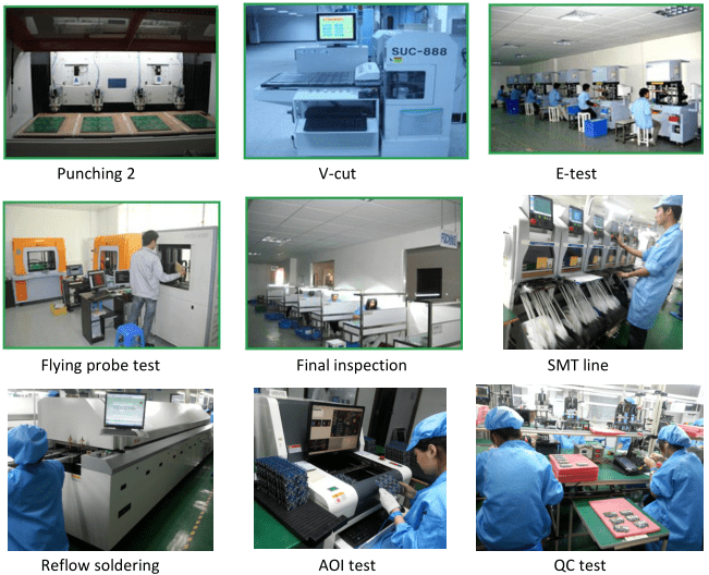
1. Three Forks Where PTFE Leaves the FR-4 Playbook
Most of the FR-4 process chain survives on F4BM220 intact: imaging, etch, solder mask, legend, electrical test. Three steps do not survive untouched. First, hole-wall preparation: PTFE is chemically inert, so a plasma or sodium-naphthalene desmear is not an option but a requirement — skip it and the electroless copper peels. Second, pressing: the F4B bonding system flows at 260–300 °C, far above an FR-4 press cycle, and hybrid stackups need the two chemistries sequenced, not merged. Third, mechanical handling: PTFE creeps under sustained load and pressure, so storage, fixturing and thin-core transport all carry rules an FR-4 line has never needed. Everything else in this page hangs off those three forks. The family context — where F4BM220 sits among the F4B grades — is mapped in the F4B family overview.
One identity note first: F4BM220 is woven-glass-reinforced PTFE clad with ED copper — the 2.20 Dk grade of the F4B family. It is not ceramic-filled (that is F4BTM), and where ultra-low PIM matters, the RTF-copper sibling F4BME swaps the foil without changing the process below. The material identity is laid out in the F4BM220 introduction; here we stay on the production floor.
2. The Process Map: FR-4 vs PTFE, Step by Step
The table below is the working summary — every row is expanded in the sections that follow.
| Process step | FR-4 default | F4BM220 (PTFE) | Why it differs |
|---|---|---|---|
| Panel storage | Rack, stack freely | Flat, unloaded; no edge clamping | PTFE cold-flows under sustained pressure |
| Drilling | Standard carbide, high aspect OK | Sharp tools, aspect ratio ≤6:1 | Soft resin smears easily; Z-CTE 240 strains plated barrels |
| Desmear | Permanganate | Plasma or sodium naphthalenide | PTFE is chemically inert — wet chemistry will not anchor copper |
| Electroless Cu | Standard line | 45–50 °C bath, slower deposition | Activation must survive on a low-energy surface |
| Etch / lines | Commodity | Same, but tolerance matters more | ±25 µm on a 0.79 mm line is ±2.8 % impedance |
| Lamination | 170–190 °C prepreg | 260–300 °C FEP bond system | Different chemistry; hybrid stacks are sequenced |
| Surface finish | ENIG default | OSP or immersion silver preferred | Nickel’s 1.33 µm skin depth dominates 10 GHz loss |
| Routing | Any method | Mechanical only; no laser | PTFE decomposes above ~400 °C, releasing fluorinated gas |
3. Incoming Material and Panel Handling
F4BM220 ships in 0.1–12 mm thicknesses on 460×610 and 914×1220 mm sheets. Two handling rules protect yield before any chemistry starts. Store panels flat and unloaded — PTFE creeps under its own weight when stacked on edge or clamped at the grip line, and a 0.25 mm core that took a set in storage will not flatten in a press. Cut with a rough blank 3–5 mm oversize, let the panel relax, then finish to size; and do not water-cool the cut — the low water absorption (≤0.08 % per the third-party datasheet figure, confirm on the lot you buy) is no license to soak the panel before bake-out.
Peel strength (≥18 N/cm), solder-dip endurance (260 °C for 20 s, no blister) and warpage (≤0.03 mm/mm at 0.25 mm) come straight from the material spec — use them as incoming-inspection gates, not as process targets. The full parameter table with design context is in the F4BM220 specifications page.
4. Drilling: Geometry Decided Here, Quality Lost Here
Mechanical drilling only — the laser question is closed by chemistry, since PTFE decomposes above roughly 400 °C and a CO₂/UV laser exceeds that locally while releasing fluorinated compounds. The numbers that decide hole quality:
| Parameter | Working rule | Consequence if missed |
|---|---|---|
| Aspect ratio | ≤6:1 for plated through-holes | Z-CTE 240 ppm/°C stretches the barrel ~83 µm on a 1.6 mm board across reflow — high aspect cracks corners |
| Tool condition | Sharp, fresh-entry tools, conservative in-feed | Soft PTFE smears at lower temperatures than FR-4; smear buries the via |
| Backer / entry | Standard entry + phenolic backup | Burrs on a soft resin pull out copper at the surface |
| Hole-size accounting | Finished hole = drill − 2×25 µm plating | Ordering 0.30 mm finished with a 0.30 mm drill delivers 0.25 mm |
The Z-CTE strain is the hidden killer. Across a 215 °C reflow swing a 1.6 mm F4BM220 board grows about 83 µm in thickness — the plated barrel must elongate with it, which is why the plating spec in the next section insists on ductile copper.
5. Desmear and Metallization: Where PTFE Cannot Be Cheated
FR-4 desmears in permanganate because the resin itself is reactive enough to texture. PTFE is not: nothing wet wets it until the surface is attacked deliberately. The two accepted routes are plasma desmear and sodium naphthalenide (sodium-naphthalene in THF), which strips fluorine from the surface and leaves a carbonizable, bondable skin. Both work; both have windows — over-treat and the glass cloth degrades, under-treat and the electroless copper lifts in solder. Treat, rinse, and plate within the same session; a treated wall left overnight re-inerts.
Electroless copper runs at 45–50 °C depositing 2–3 µm/h. For high-aspect voltage on thin cores, the panel-plating ratio matters: a 5:1 deep barrel wants ~42 µm of surface copper to guarantee coverage at the knee, and the finished plating must be ductile (≥20 % elongation class) to survive the Z-expansion above. This is also the step where a first-article coupon earns its keep — cross-section the knees before the batch runs.
6. Etch and Line Geometry at RF Tolerances
Etching F4BM220 is ordinary chemistry on an extraordinary tolerance budget. At the reference design point — 0.254 mm core, 50 Ω — the line is 0.79 mm wide, and a ±25 µm etch band moves impedance ±2.8 %. On a 0.127 mm core the line drops to 0.40 mm and the same ±25 µm is ±5.5 % — which is why thin-core RF builds go coupon-verified rather than datasheet-verified. Watch undercut on heavier copper: at 2 oz the 28 µm per-side etch signature makes sub-0.15 mm lines a knife-edge, so 2 oz and fine pitch should not share a design.
The impedance-control workflow — stackup review, coupon design, TDR verification — is the same as any RF build and is detailed in the impedance control guide. The F4BM220-specific note: solder mask over bare PTFE pulls measured impedance down 1–3 Ω (mask Dk sits well above 2.20), so the coupon that matches the drawing is the bare-coupon one.
7. Multilayer and Hybrid Pressing: Two Chemistries, One Stack
F4B bonding runs in the 260–300 °C window (FEP film or low-flow prepreg) — an FR-4 press cycle (170–190 °C) will not bond it, and a PTFE cycle will degrade FR-4. Hybrid stackups therefore press in sequence, not in one cycle; the full temperature-pressure schedule is worked through in the hybrid lamination guide. Three numbers control the RF outcome:
| Factor | Number | Effect on the RF build |
|---|---|---|
| Bondply thickness | ~0.10 mm typical | Forgotten in the stackup, a 50 Ω microstrip lands at ~61 Ω (+22 %) |
| Prepreg shrinkage | 0.02–0.05 % | 0.12–0.30 mm layer-to-layer misregistration on a 600 mm panel |
| Press-induced thinning | ~4 % on over-thick bond | A PTFE core pressed thin shifts every impedance in the stack |
Post-press relaxation before routing follows the same rule as panel cutting: PTFE remembers pressure. A board routed hot off the press drifts; one rested flat for hours does not.
8. Surface Finish: The Cheapest dB You Will Ever Buy
At 10 GHz the copper skin depth is 0.65 µm — thinner than any ENIG nickel layer, so the RF current in an ENIG pad flows entirely in nickel, whose rougher surface conductivity costs roughly 2× the resistance of copper. On a material bought for Df 0.0010, that makes finish selection a first-order loss decision: OSP is the lowest-loss route, immersion silver next, ENIG acceptable where solderability or wire bonding forces it. The same logic applies to legend ink — white ink sits near Dk 6.5 over 50 Ω lines, so mark it off the RF path, not over it.
Where the loss budget is being argued at system level, the numbers are in the industry applications page — the finish decision there changes tenths of a dB per inch, not hundredths.
9. Inspection Gates and the Records Worth Keeping
Acceptance runs to IPC-A-600G / IPC-6015 class criteria. The gates specific to F4BM220: cross-section through-hole knees (plating thickness and ductility, post-desmear adhesion), coupon TDR against the stackup (bare coupon vs finished-board delta documented), solder-float witness coupons at 260 °C/20 s against blistering, and warpage after final rout. Because the material’s TCDk is −142 ppm/°C — about 2.8 % Dk drift over a 200 K swing, not “stable under temperature variations” as some listings claim — keep the press and desmear lot records with the coupon data: when a field unit drifts, the question is process, not material, and only the records answer it.
10. What the Source Page Got Wrong, Itemized
The article this page replaces carried four claims worth flagging, since variants of them circulate on dealer sites:
| Claim in circulation | Correction |
|---|---|
| “TCDk −142 … performance remains stable under temperature variations” | Direction reversed: −142 ppm/°C is a large drift (5880-class). Budget the phase or step to a filled grade |
| “Water absorption ≤0.02 %” | Third-party datasheet figure is ≤0.08 % — still excellent, but quote the document you can defend |
| “Major manufacturer: Shenzhen Xincheng’er Electronics” | Role confusion: the laminate is made by Wangling (F4B maker); XCE is a PCB fabricator. Laminate data comes from the laminator’s datasheet |
| “ED copper foil” as the only option | F4BME substitutes RTF foil for low-PIM builds — same process chain, different foil |
11. Handing a Stackup to the Floor: The RFQ Fields That Matter
A fabrication-ready RFQ for F4BM220 carries: core thickness and foil weight per layer, the bondply included in the stackup math, foil type (ED vs RTF), finished hole sizes with the drill complication understood, target impedance with bare-coupon acceptance, surface finish with the loss argument stated, and solder-mask-off zones over RF lines. Custom lamination (mixed F4B grades, hybrid with FR-4) is routine — XCE builds PTFE and hybrid boards in-house with desmear, pressing and coupon verification under one roof, 600×1200 mm capability, impedance ±10 % standard and ±3 % coupon-verified, samples in as fast as 24 hours, inspected to IPC-A-600G and IPC-6015, with 80+ engineers on 10,000+ builds since 2009. Send the stackup and the band, and the process plan comes back with the quote. Where the argument turns to money, the cost-structure breakdown shows which process steps actually move the price.
Frequently Asked Questions
Does F4BM220 need sodium naphthalene treatment, or is plasma enough?
What aspect ratio is safe for plated through-holes in F4BM220?
Can F4BM220 be laser-drilled or laser-cut?
Why does surface finish matter more on this material than on FR-4?
Can F4BM220 be pressed together with FR-4 in one cycle?
What should an incoming inspection on F4BM220 check?
Send the Stackup for a Fabrication Review
Send us your Gerber files and requirements for a manufacturability review and a tailored quotation.
sales1@xcepcb.com
+86 180 3341 4657