
Most F4BM220 pcb pages copy the same parameter block — and most copies carry three wrong numbers. This is the design-engineer version: the corrected official parameters, the 50 Ω line-width arithmetic on every standard thickness, and the tolerance stack that links dielectric thickness to final impedance — the three things a stack-up actually consumes before the board goes to fabrication.
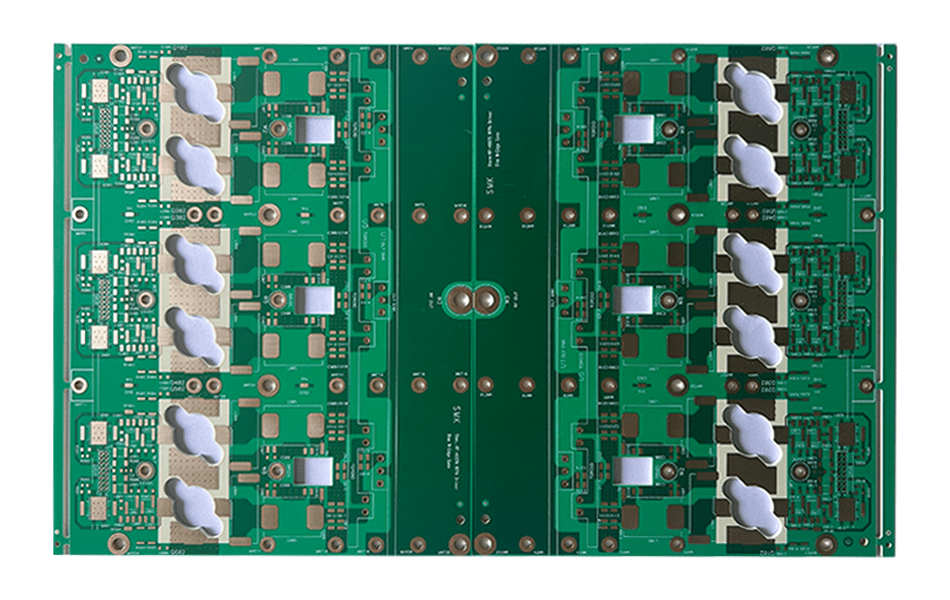
F4BM220 is the Dk 2.20 grade of the F4B family: PTFE resin on woven glass cloth, electrodeposited copper. The parameters below are the manufacturer’s published values; the right column lists what most secondary sources print instead, because the same three errors circulate from page to page:
| Parameter | Official value | Often quoted as | Why the difference matters |
|---|---|---|---|
| Dk @10 GHz | 2.20 ± 0.04 | 2.2 ± 0.02 | The real tolerance is twice the claimed one — it feeds straight into the impedance budget (section 3) |
| Df @10 GHz | 0.0010 | 0.0009 | 0.0009 is RT/duroid 5880’s figure; F4BM220 is 0.0010 — the loss budget shifts by 10 % |
| CTE, x / y | 25 / 34 ppm/°C | 16 / 16 | Affects registration against copper across thermal cycling |
| CTE, z | 240 ppm/°C | 24 | Off by 10×; changes via design completely (section 5) |
| TCDk | −142 ppm/°C | “stable” | A large negative coefficient — phase-critical designs must budget it |
| Water absorption | ≤0.08 % (24 h) | ≤0.02 % | Confirm the figure for your thickness from the current datasheet |
Everything else on the datasheet — UL 94 V-0 rating, peel strength ≥18 N/cm, 260 °C solder-dip survival, thickness from 0.1 to 12 mm — is consistent across sources. The naming, and where this grade sits among the nine F4BM rungs, is in the F4B family map.
With the Dk fixed, microstrip geometry follows. The W/h ratio for 50 Ω on Dk 2.20 is 3.11 with an effective permittivity of 1.87, so every standard thickness produces a definite line width — and a definite sensitivity to etch error, because the same ±25 µm etch tolerance is a different fraction of each width:
| Dielectric h | W for 50 Ω | Etch ±25 µm → Z error | h ±10 % → Z error | Design note |
|---|---|---|---|---|
| 0.127 mm | 0.40 mm | ≈±5.5 % | ≈±6 % | mmWave builds; every µm of etch control is worth real impedance |
| 0.254 mm | 0.79 mm | ≈±2.8 % | ≈±6 % | The workhorse thickness for RF front ends |
| 0.508 mm | 1.58 mm | ≈±1.4 % | ≈±6 % | Lower-loss builds; wider filters and couplers |
| 1.0 mm | 3.11 mm | ≈±0.7 % | ≈±6 % | Power feeds; etch is no longer the limiting term |
Two patterns to take from the table. First, thickness tolerance is the dominant term at every thickness — the ±10 % laminate window moves impedance about as much as everything else combined, which is why the coupon exists (section 3). Second, etch sensitivity falls eightfold from the thinnest to the thickest row: a 0.127 mm build needs tighter etch compensation than a 1 mm build by definition, not by vendor skill. The impedance model behind these numbers, including the solder-mask offset, is in the high-frequency impedance control guide.
A ±10 % tolerance on dielectric thickness translates to roughly ±6 % on 50 Ω impedance — the single largest term in the budget. Stack the published tolerances for the 0.254 mm build and the picture is:
| Term | Tolerance | Z contribution (0.254 mm build) |
|---|---|---|
| Dielectric thickness | ±10 % | ≈±6 % |
| Etched line width | ±25 µm | ≈±2.8 % |
| Dk spread | ±0.04 on 2.20 | ≈±0.4 % |
| Solder mask | 20–30 µm over the line | −1 to −3 Ω on the finished board |
Note what the Dk row does not do: even the full ±0.04 grade tolerance moves impedance by well under one percent — on this material, geometry tolerance dominates material tolerance. That is why an impedance window is proven with a coupon on the same panel: same stack, same copper weight, same press cycle, TDR-measured per layer. The standard window is ±10 %; ±3 % is achievable but only with a coupon-verified build and usually one etch re-compensation. Acceptance measurements belong in the plan from the start — the testing checklist lists what to measure on first articles.
Df 0.0010 puts the dielectric loss of a 50 Ω F4BM220 line at 0.039 dB/inch at 10 GHz — 28 times better than FR-4’s 1.08. But the honest loss budget adds the conductor, and at these Df levels the conductor is no longer small:
| Frequency | Dielectric loss αd | Total, 1 oz Cu | Where the rest goes |
|---|---|---|---|
| 10 GHz | 0.039 dB/in | ≈0.23 dB/in | Copper roughness and finish carry the rest — ≈5× the dielectric |
| 28 GHz | 0.109 dB/in | ≈0.7 dB/in | Skin depth shrinks; roughness and nickel finishes dominate |
The design consequence: once the dielectric is this good, surface finish choice moves more dB than laminate choice. ENIG buries the 10 GHz current in nickel, roughly doubling the conductor loss; OSP or immersion silver keep the current in copper. On FR-4 the material decision is 90 % of the budget; on F4BM220 it is the finish, the copper profile and the mask. The 5880 comparison — same Dk class, Df 0.0009 — is quantified in the RT/duroid 5880 analysis.
Three thermal numbers from the corrected table turn into three design rules, and the Z-CTE one is the reason PTFE-class boards are built differently:
| Number | Value | Design rule it produces |
|---|---|---|
| TCDk −142 ppm/°C | Dk −2.8 % over 200 K | Phase-matched structures: budget ≈24° per 100 mm at 10 GHz, or climb the ladder to F4BM300 (−80) |
| Z-CTE 240 ppm/°C | 1.6 mm grows ≈83 µm in reflow | Aspect ratio ≤6:1, high-elongation plating; count reflow cycles as a finite resource |
| Thermal conductivity ≈0.2–0.25 W/(m·K) | Poor conductor of heat | High-power sections need thermal vias and copper coins — the laminate will not spread heat |
The third row corrects another circulating claim: PTFE-glass laminates are sometimes pitched as “ideal for high-power heat dissipation”. At 0.2–0.25 W/(m·K) they are roughly a hundred times worse than aluminium — the material’s thermal job is to stay out of the way, and heat exits through vias, coins and copper pour, not through the dielectric. What the Z-CTE row means for manufacturing — desmear chemistry, plating windows, press cycles — is the subject of the F4BM220 processing page.
Three environmental facts round out the specification. Moisture: with water absorption at or below 0.08 %, Dk movement from humidity is small enough that indoor storage and normal assembly humidity are non-events — the number to protect is the coupon-impedance budget, not the laminate. Chemistry: PTFE is inert to the acids, alkalis and solvents that attack epoxy systems, which is why F4B boards survive cleaning chemistries and industrial atmospheres that age FR-4. Storage: the one handling rule that differs from FR-4 is cold flow — unreinforced PTFE creeps under sustained point loads, so panels are stored flat without stacked weight or edge clamping, and thin cores are handled at the edges.
Compliance paperwork (RoHS, REACH) comes with the laminate datasheet; fabricator-side compliance — finish chemistry, solder mask, peel and ionic cleanliness — comes with the board quote. The two documents answer different audits, and the fabricator can supply both for a single part number.
The previous version of this page carried the standard copy-paste parameter block. For the record, the five corrections with their sources:
| Old claim | Corrected | Basis |
|---|---|---|
| “Dk 2.2 ± 0.02” | 2.20 ± 0.04 | Manufacturer published table |
| “Df 0.0009” | 0.0010 | Manufacturer published table (0.0009 is 5880) |
| “CTE z 24 ppm/°C, good match to copper” | Z-CTE 240 | Manufacturer data; 240 is 14× copper — the opposite of matched |
| “Ideal for high-power heat dissipation” | ≈0.2 W/(m·K), poor | PTFE class thermal conductivity; heat exits via vias and coins |
| “MRI and CT imaging systems” | Removed | Imaging RF sits at 64–298 MHz where FR-4 is already adequate; the real medical drivers are repeatability and build stability |
Where the applications that do hold up are listed by industry — and why each industry picks 2.20 — is the subject of the F4BM220 industries page.
For a stack-up that uses F4BM220, five decisions close the design before quoting, and each maps to a section above:
One. Fix the impedance window — ±10 % standard, ±3 % coupon-verified (section 3). Two. Pick thickness for etch sensitivity, not just for loss: 0.127 mm buys low loss and sells tolerance pain (section 2). Three. Choose the finish for the frequency — nickel-free above ~10 GHz where the budget is tight (section 4). Four. Design the vias for Z-CTE 240: aspect ratio ≤6:1, ductile plating, reflow count budgeted (section 5). Five. If phase matters across temperature, either budget the 24° or step up the ladder — the Dk cost of F4BM300 is about 18 % narrower traces for half the drift (section 5).
With those five closed, the quote that comes back is comparable and the coupon will prove it. The first-order introduction to the material, if the stack-up is being written from scratch, is in the F4BM220 introduction, and the full model list including the RTF-copper and ceramic-filled branches is in the sheet model list.
F4BM220 spec-by-spec: Dk 2.20 ± 0.04 with effective permittivity 1.87, so a 50 Ω line is 0.79 mm on the 0.254 mm workhorse core; Df 0.0010 for 0.039 dB/inch of dielectric loss at 10 GHz against ≈0.23 dB/inch total, where the finish outweighs the laminate; TCDk −142 and Z-CTE 240 as the two numbers that set phase budgets and via rules respectively; and a tolerance stack in which thickness, not material spread, is the dominant term — hence the coupon.
XCE PCB builds F4BM220 stacks to that arithmetic: 2 to 72 layers, panels to 600×1200 mm, impedance ±10 % standard and ±3 % coupon-verified, PTFE desmear and hybrid pressing in-house, samples in as fast as 24 hours, 5,000 m² of plant with 80+ engineers and over 10,000 high-frequency builds since 2009, inspected to IPC-A-600G and IPC-6015. Send the stack-up and the impedance window, and the coupon plan comes back with the quote.
Send us your Gerber files and requirements for a manufacturability review and a tailored quotation.