
The Rogers 4000 PCB series is usually presented as a list of part numbers, which hides the more useful fact: every RO4000 material is the same chemistry — glass-reinforced hydrocarbon with ceramic filler, a thermoset rather than PTFE — and that single decision is what makes the whole family drill, plate, laminate and etch on an FR-4 line. What changes between the branches is mostly dielectric constant, flame rating and copper foil. This article covers the platform, not the catalogue.
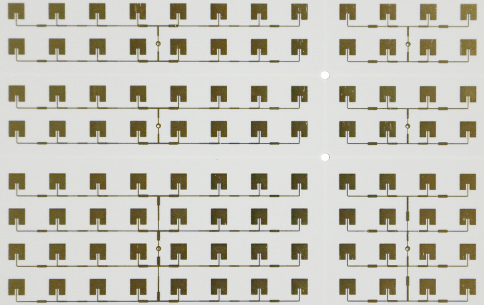
A Platform, Not a Catalogue
The RO4000 family is often described as though each part number were a separate material. In fact all of them are the same construction: a woven glass fabric impregnated with a hydrocarbon resin loaded with ceramic powder, cured as a thermoset. Dk is then tuned by the filler loading, flame rating by the resin chemistry, and copper roughness by which foil is bonded to it. Nothing else changes the physics.
That matters because the platform is where the value is. Because the resin is a thermoset and not PTFE, RO4000 laminates drill with standard carbide tooling, desmear in permanganate, take standard solder mask and plate in a conventional electroless copper line. Because the resin is hydrocarbon rather than epoxy, the dissipation factor is 0.0027–0.0038 instead of FR-4’s 0.020. The combination — RF-grade loss on an FR-4 line — is the entire commercial argument, and it is why the family has stayed the default choice for base-station, radar and antenna work for two decades.
Where the argument breaks is at the edges: the press window, the flame rating, the peel strength and the thermal expansion in Z. Those four are the subject of most of what follows.
What the Family Actually Contains
Rogers publishes eight product lines under RO4000. Reading them as a map rather than a list makes selection much faster, because each line answers a different question.
| Line | What it answers | Defining number |
|---|---|---|
| RO4003C | Cheapest route to RF loss without a flame requirement | Dk 3.38 ±0.05, Df 0.0027 |
| RO4350B | Same platform with a UL 94 V-0 rating; the volume workhorse | Dk 3.48 ±0.05, Df 0.0037 |
| RO4835 | Oxidation resistance for long-life and high-humidity assemblies | Dk 3.48, Df 0.0037, 10× oxidation resistance |
| RO4360G2 | Size reduction at high Dk on the same process | Dk 6.15 ±0.015, Df 0.0038 |
| RO4400 / RO4400T | Bondply for multilayer and sequential lamination | Matched to the core family |
| RO4500 | Commercial antenna grade, high volume | Antenna-grade economics |
| RO4700 | Low-Dk antenna grade with low PIM | Dk 2.55 or 3.00, Df 0.0022 at 2.5 GHz |
| RO4000 LoPro / CU4000 | Reverse-treated foil for lower loss and lower PIM | Foil, not laminate |
Two entries are not laminates at all — RO4400 is bondply and CU4000 is foil — and it is common to see a specification that asks for “RO4350B” when what was meant was a stack-up of 4350B cores bonded with 4450B prepreg. Getting that distinction right is worth more than any parameter comparison, because the bondply determines the finished dielectric height and therefore the impedance.
The Chemistry That Sets Everything Else
Hydrocarbon resin, ceramic filler, woven glass. Each of the three does one job, and the jobs explain the parameter set.
The hydrocarbon resin is what makes the loss low. Epoxy carries polar hydroxyl groups that rotate in the field and absorb energy; a hydrocarbon backbone does not, so Df falls by nearly an order of magnitude — from 0.020 to 0.0027–0.0038 — without any change in how the board is made. It is also why the material is a thermoset: the resin cross-links during the press, so the dielectric does not cold-flow under clamping pressure the way PTFE does.
The ceramic filler raises Dk and lowers thermal expansion. It is also the reason Dk can be sold from 2.55 to 6.15 on the same chemistry: change the loading, change the dielectric constant. The cost is that a filled resin is abrasive, which shows up as drill wear rather than as an electrical problem.
The glass fabric gives the mechanical properties — dimensional stability, peel, drillability — and it also introduces the one artefact designers notice: Dk varies slightly between glass bundles and resin-rich areas. On fine features the weave becomes visible as impedance ripple, which is why spread-glass and thin-core variants exist for high-density work.
One Dk Range, Two and a Half Times Apart
Because the filler loading is the tuning knob, the family spans Dk 2.55 to 6.15. That range is not cosmetic: guided wavelength scales as 1/√Dk, so the same circuit is 40 % smaller at 6.15 than at 3.48, and 36 % larger at 2.55.
| Dk | Family member | 50 Ω W/h | Guided wavelength at 10 GHz | Relative circuit area | Df |
|---|---|---|---|---|---|
| 2.55 | RO4700 antenna grade | 2.94 | 20.3 mm | 1.36 | 0.0022 at 2.5 GHz |
| 3.00 | RO4700 antenna grade | 2.54 | 19.3 mm | 1.16 | 0.0023 at 2.5 GHz |
| 3.38 | RO4003C | 2.33 | 18.4 mm | 1.03 | 0.0027 |
| 3.48 | RO4350B / RO4835 | 2.27 | 18.2 mm | 1.00 | 0.0037 |
| 6.15 | RO4360G2 | 1.55 | 14.2 mm | 0.61 | 0.0038 |
The insight in that table is the last column pair. Going from 3.48 to 6.15 takes 39 % off the area and adds 0.0001 to Df — nothing. Dielectric loss per unit of electrical length is essentially unchanged, because it depends on Df and not on Dk. So high Dk within this family is a size decision, never a loss decision, and a design that needs lower loss has to leave the platform entirely: RT/duroid 5880 at Df 0.0009 is the material for that job, at roughly three times the laminate cost and with a very different fabrication flow.
Two Dk Numbers, and Why Designs Land Off Target
Every RO4000 data sheet carries two dielectric constants: a process value measured on a clamped stripline at 10 GHz, and a design value used for impedance calculation across the 8–40 GHz band. They are not the same number, and the gap is not a rounding error.
| Material | Process Dk (10 GHz) | Design Dk (8–40 GHz) | Difference | 50 Ω error if the wrong one is used |
|---|---|---|---|---|
| RO4003C | 3.38 ±0.05 | 3.55 | +5.0 % | about 1.3 % — 50.0 becomes 49.4 Ω |
| RO4350B | 3.48 ±0.05 | 3.66 | +5.2 % | about 1.3 % |
| RO4835 | 3.48 ±0.05 | 3.66 | +5.2 % | about 1.3 % |
1.3 % looks harmless in isolation and is not, because it is a bias rather than a scatter: every line on the board moves the same way, and it stacks with the two larger terms. Thickness at ±10 % contributes ±6 % to impedance; etch at ±25 µm contributes ±2 % on a 0.59 mm line. Add a one-directional 1.3 % and a ±5 % window has no margin left for the fabricator.
There is a second trap on thin cores. Rogers footnotes the 0.101 mm (4 mil) build of 4350B at Dk 3.36 and of 4835 at 3.33, below the standard process value. A 4-mil design copied from a 10-mil stack therefore runs high in impedance by roughly 1.5 %, and no amount of etch control recovers it. When the stack mixes thicknesses, the coupon should be built on the same core thickness as the product.
“FR-4 Compatible” and Where It Stops
The compatibility claim is true and is routinely over-read. Eight process steps behave the same, four do not.
| Step | Same as FR-4? | What to watch |
|---|---|---|
| Drilling | Yes | Ceramic filler is abrasive; tool life is shorter, hole quality is fine |
| Desmear | Yes | Permanganate works — the single biggest advantage over PTFE, which needs sodium naphthalenide or plasma |
| Electroless copper / plating | Yes | Standard line; no special activation |
| Solder mask and legend | Yes | Standard epoxies adhere well because the surface is not PTFE |
| Lamination temperature | No | 190–200 °C against 170–190 °C for FR-4, so the two cannot be co-cured in one press |
| Peel strength | No | 0.88–1.05 N/mm, about 60–75 % of FR-4; pad design and rework limits must reflect it |
| Z-axis CTE | No | 32–46 ppm/°C, two to three times copper; not a “matched” material in Z |
| Flame rating | Depends | 4003C carries no UL 94 rating; 4350B and 4835 are V-0. This decides more projects than Df does |
The lamination row is the one that costs money. A mixed RO4000/FR-4 board has to be pressed in two cycles or bonded with RO4400 prepreg in a sequenced flow; a fabricator who quotes it as a single press will either fail the FR-4 cure or over-cure the hydrocarbon. That sequencing, not the raw material price, is where hybrid boards get expensive.
CTE in Three Axes: One Advantage, One Trap
The original version of this article claimed that RO4000’s thermal expansion “closely matches copper”, which is half right and half dangerously wrong. In plane it is better than matched; through the thickness it is two to three times copper.
| Material | X | Y | Z | Z relative to copper (17) | Expansion of 1.6 mm across 215 K |
|---|---|---|---|---|---|
| RO4003C | 11 | 14 | 46 | 2.7× | 15.8 µm |
| RO4350B | 10 | 12 | 32 | 1.9× | 11.0 µm |
| RO4835 | 10 | 12 | 31 | 1.8× | 10.7 µm |
In plane, 10–14 ppm/°C is below copper’s 17, which is the useful direction: the laminate shrinks less than the foil that is bonded to it, so the copper is in slight compression rather than tension, and registration at sequential lamination stays predictable. That is the real content of the “dimensional stability” claim.
In Z, 32–46 ppm/°C against 17 for copper means the plated barrel absorbs 11–16 µm of differential movement on a 1.6 mm board through a lead-free reflow. That is survivable with high-ductility plating, and it is one of the better figures in the industry — PTFE laminates run 200–240 ppm/°C and move 75–82 µm — but it is not matching, and a stack-up note that says “CTE matched to copper” without an axis is a note that will be misread.
Flame Rating Against Loss: You Cannot Have Both
The single most consequential pair of numbers in this family is 0.0027 with no flame rating against 0.0037 with V-0. The gap is not a manufacturing accident; it is chemistry. A V-0 rating needs brominated or phosphorus-based flame retardants, and those additives are polar, so they raise the dissipation factor.
| Property | RO4003C | RO4350B | Consequence |
|---|---|---|---|
| UL 94 | No listed rating | V-0 | Decides whether the board can ship into many end products at all |
| Df at 10 GHz | 0.0027 | 0.0037 | 37 % more dielectric loss |
| Dielectric loss at 10 GHz | 0.13 dB/in | 0.18 dB/in | 0.05 dB/in; copper still dominates the total |
| Total microstrip, 0.254 mm, 1 oz | 0.32 dB/in | 0.38 dB/in | 19 % on the whole line, not 37 % |
| Peel strength | 1.05 N/mm | 0.88 N/mm | The flame-retarded version bonds less well |
Put that way, the choice is usually made for you: if the product needs V-0, 4003C is not a candidate regardless of its loss, and the honest comparison is 4350B against a different platform rather than against its own sibling. This is also why the two materials are so often described in the wrong order — 4003C is not the “better” grade, it is the grade without the additive. The full side-by-side is in the 4350B and 4003C comparison.
The Antenna Branch: RO4700
Antenna work has requirements this platform meets awkwardly at Dk 3.4: passive intermodulation has to be low, weight matters on a mast, and cost is set by square metres rather than by performance. The RO4700 line answers all three by dropping Dk to 2.55 or 3.00.
The lower Dk does two things at once. It widens every 50 Ω line, which reduces conductor loss and makes etch tolerance a smaller fraction of the width; and it moves the design closer to air, which is where a radiating element wants to be. PIM falls as well, partly from the lower Dk and partly from the reverse-treated foil used in these grades — PIM is a surface phenomenon and a smooth foil interface is the cheapest way to improve it.
The trade is size: 36 % more area at Dk 2.55 than at 3.48, which on an antenna panel is paid for in mechanical structure rather than in laminate. For a base-station array that is often the right trade, since the panel is a fixed mechanical envelope anyway.
Sequential Lamination and Hybrid Stack-ups
RO4400 bondply exists because cores alone cannot make a multilayer. The prepreg is the same chemistry in a B-stage, so it cures in the same 190–200 °C press and does not introduce a second dielectric system with its own Dk.
Three rules govern the stack. The bondply thickness counts toward the dielectric height, so an impedance calculation that uses the core thickness alone is wrong by the bondply on both faces of the layer — on a 0.254 mm core with 0.10 mm of prepreg, a 50 Ω line designed on 0.254 mm lands closer to 61 Ω. The press window cannot be shared with FR-4, so a hybrid board is either pressed twice or designed with the FR-4 as a cured sub-assembly. And sequential lamination needs a bake between cycles to remove the stress that etching leaves in the laminate, or the inner layers move during the second press.
Hybrid boards are where most of the cost and almost all of the schedule risk live. A pure RO4000 stack is a straightforward build on an FR-4 line; an RO4000 plus FR-4 stack is a process design exercise, and the discussion in the RO4350B and RO4835 commercial guide covers the platform-level part of it.
What the Platform Costs
Laminate cost for this family runs about three to five times standard FR-4 per square metre. That number is quoted often and understood rarely, because the laminate is a small part of a finished board: on a six-layer mixed build, material is typically 20–30 % of the price, so a 4× laminate becomes a 1.6–2× board — and if the board is small and the quantity large, the RF material only needs to occupy the layers that carry RF.
That last point is the real cost lever, and it is a design decision rather than a purchasing one. Putting the antenna and the feed on RO4000 and the digital and power distribution on FR-4 usually beats converting the whole stack, provided the hybrid rules in the previous section are respected. Converting everything to RF material buys uniformity and pays for it on layers where Df never mattered.
Choosing Within the Family
| Requirement | Start with | Because |
|---|---|---|
| Lowest loss, no flame requirement, cost sensitive | RO4003C | 0.0027 is the family floor |
| Flame rating required, general RF | RO4350B | V-0 at 0.0037, the widest process experience |
| Long field life, humid or hot environment | RO4835 | 10× oxidation resistance, electrically equivalent to 4350B |
| Size is the constraint, loss is not | RO4360G2 | Dk 6.15 gives 39 % less area at the same Df |
| Base-station antenna, low PIM, weight matters | RO4700 series | Dk 2.55–3.00, Df 0.0022, lighter panels |
| Millimetre wave, 60–81 GHz industrial radar | RO4835IND LoPro | Reverse-treated foil; above 30 GHz foil roughness outweighs Dk |
| Below 0.002 in Df, or phase-critical over temperature | Leave the platform | PTFE materials — RT/duroid 6002 or RO3003 |
The last row is the one that saves the most time. No amount of work within RO4000 gets below 0.0027, because the floor is set by the resin chemistry; if the link budget needs Df 0.0010 or better, the answer is a different platform with a different fabrication flow, which is a project decision and should be made before the stack-up is drawn.
Conclusion
The Rogers 4000 series is one material system sold in eight forms. The constant is a glass-reinforced hydrocarbon thermoset with ceramic filler that drills, desmears, plates and laminates on an FR-4 line at Df 0.0027–0.0038. The variables are Dk from 2.55 to 6.15, a flame rating that exists on some grades and not others, and which copper foil is bonded to the surface.
Three corrections matter more than the parameter list. The expansion matches copper in plane — 10–14 against 17, which is a registration advantage — and runs two to three times copper in Z, at 32–46, which is a via-strain account. The thermal conductivity of 0.66–0.71 W/m·K is roughly twice FR-4 and not a heat-spreading solution. And the loss floor of 0.0027 belongs to the grade without a flame rating, so V-0 and the lowest loss in the family are mutually exclusive by chemistry.
XCE PCB runs this platform and the PTFE platforms on the same floor: 2 to 72 layers, panels to 600×1200 mm, impedance ±10 %, samples in as fast as 24 hours, inspected to IPC-A-600G and IPC-6015. Sequenced hybrid lamination with RO4400 prepreg and coupon verification per core thickness are standard, because on this family the stack-up, not the part number, decides whether the impedance lands. For the model-by-model parameters, see the RO4350B selection guide and the 4350B against 4835 comparison.
Frequently Asked Questions
Is Rogers 4000 series PTFE?
What is the dielectric constant range of the RO4000 family?
Why do RO4003C and RO4350B have different loss if they are the same platform?
Does the CTE of RO4000 match copper?
Can RO4000 be laminated together with FR-4?
Which Dk should I use for impedance calculation?
Need RO4000 and FR-4 in the Same Build?
Send us your Gerber files and requirements for a manufacturability review and a tailored quotation.
sales1@xcepcb.com
+86 180 3341 4657