
Most high-frequency laminates are thermal insulators: 0.2–0.7 W/m·K, which is why RF boards move heat with via arrays rather than through the dielectric. RT/duroid 6035HTC breaks the pattern at 1.44 W/m·K — about 2.4 times the standard RT/duroid 6000 materials — while keeping Dk at 3.50 and Df at 0.0013. This article explains what that conductivity is worth in kelvin, where it changes a design decision, and what the material gives up in exchange.
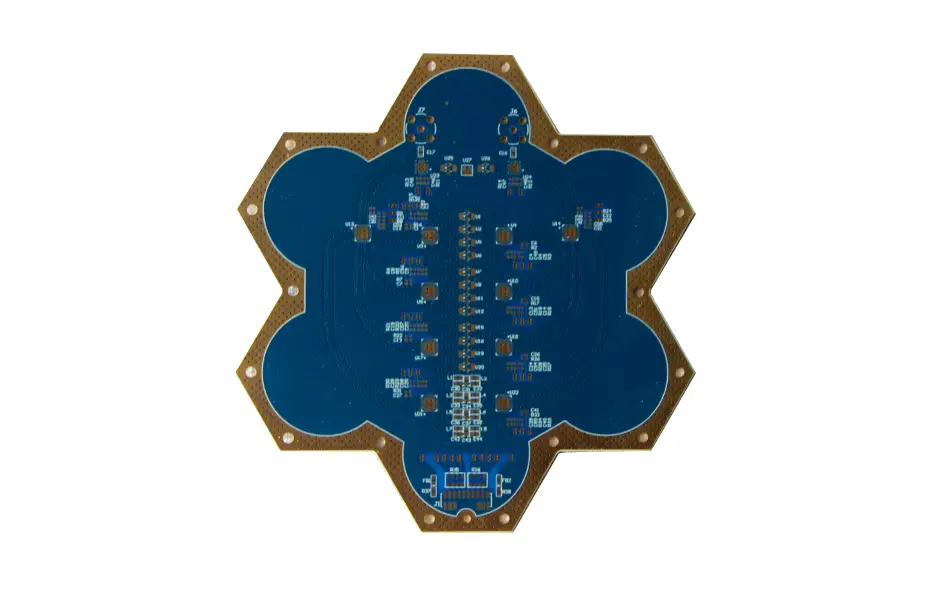
The Datasheet, Verified
RT/duroid 6035HTC is a ceramic-filled PTFE built around a high-conductivity filler system — the “HTC” is high thermal conductivity, and it is the reason the product exists.
| Property | RT/duroid 6035HTC | Note |
|---|---|---|
| Dk, process / design | 3.50 ± 0.05 / 3.6 | A “3.5-class” material: wide 50 Ω traces, EC-typical of 4350B territory |
| Df @ 10 GHz | 0.0013 | Low: half the loss of RT/duroid 6006 (0.0027), better than RO4350B (0.0037) by nearly 3× |
| TCDk | −66 ppm/°C (−50…150 °C) | Small in magnitude — phase drift is modest for a filled PTFE |
| CTE X / Y / Z | 19 / 19 / 39 ppm/°C | Z 39 is PTFE-like, not 5880-like (237) |
| Thermal conductivity | 1.44 W/m·K @ 80 °C | The headline; ~2.4× standard 6000 materials |
| Density | 2.2 g/cm³ | Low for a filled material |
| Moisture absorption | 0.06% | Typical PTFE composite |
| Copper peel | 7.9 pli (1.4 N/mm) | The honest weakness — lower than 6010.2LM’s 2.1 N/mm |
| Dielectric strength | 835 V/mil; 12.59 kV at 15 mil | Relevant for high-voltage bias lines on the same board |
| Tensile modulus | 329 / 244 kpsi (MD / CMD) | Stiffer than unfilled PTFE, softer than glass-reinforced |
| Flammability | UL 94 V-0 | Lead-free compatible |
What 1.44 W/m·K Is Worth in Kelvin
The useful comparison is not conductivity but thermal resistance per unit area: R″ = t/k. For a 0.254 mm dielectric layer:
| Material (0.254 mm) | k, W/m·K | R″, K·cm²/W | Rise at 10 W/cm² |
|---|---|---|---|
| RT/duroid 6035HTC | 1.44 | 1.76 | 17.6 K |
| RO4350B | 0.69 | 3.68 | 36.8 K |
| RT/duroid 6010.2LM | 0.86 | 2.95 | 29.5 K |
| FR-4 (~0.3) | 0.30 | 8.47 | 84.7 K |
| RT/duroid 5880 | 0.20 | 12.7 | 127 K |
Read the last column as the temperature difference the substrate itself imposes before any via or heatsink helps: 18 K against 37 K on a hydrocarbon laminate, 85 K on FR-4, 127 K on 5880. On a high-power amplifier with 10 W/cm² of dissipated power under the output stage, that is the difference between a junction temperature with margin and one without.
The conductivity also works laterally. Field-effect transistor cells spread heat over a few millimetres of substrate; a material that conducts 1.44 W/m·K spreads it before it reaches the vias, lowering the peak rather than just the average. That is the effect a via array cannot deliver, because vias move heat vertically and the substrate is the lateral bottleneck.
The Electrical Case Is Not an Afterthought
A thermal laminate that loses electrical performance would solve nothing — and high-conductivity filler systems usually bring loss with them. 6035HTC does not: Df 0.0013 at 10 GHz sits between the low-loss 5880-class materials and the hydrocarbons, with Dk 3.50 that keeps traces at a workable width.
Two further electrical points matter on power designs. TCDk of −66 ppm/°C is small enough that a 100 mm line drifts only a few degrees of phase across a 200 °C span — far less than the −425 of 6010.2LM — so matching networks hold their tuning as the board warms. And Z-CTE 39, while not glass-reinforced territory, limits barrel strain to about 0.28% across 125 °C: a multilayer power board is feasible, not a reliability gamble.
Where It Changes a Design Decision
- Power amplifiers at X-band and above. Where output power is limited by junction temperature and the dielectric sits directly under the die attach area.
- Solid-state transmitters and T/R modules. Arrays where dozens of small amplifiers each dissipate modest power into a shared substrate.
- Filters and combiners handling high RF power. Conductor losses become heat, and a low-loss material that also conducts keeps the resonator temperature down — which matters because Dk and dimensions both move with temperature.
- Structures combining bias and RF on one substrate. Dielectric strength 835 V/mil simplifies isolation questions.
- Boards where vias are scarce or impossible. Dense connector fields and sealing constraints can block thermal via arrays; a conductive substrate routes around the constraint.
Where it does not change anything: low-power receivers, passive antenna arrays and control boards. On those, 4350B or 5880 gives better loss per euro, and the extra conductivity buys nothing.
What It Gives Up
| Compromise | Number | Practical consequence |
|---|---|---|
| Peel strength | 7.9 pli (1.4 N/mm) | Lower than other RT/duroid materials: avoid repeated rework on the same pad; plan heavy-copper areas for single-pass assembly |
| Dk 3.50 vs 6.15 | Longer lines than a 6006-class material | Compact designs must accept larger footprints; this is not a miniaturisation material |
| Panel and thickness range | Standard 0.254 / 0.508 / 0.762 / 1.524 mm; panels 305×457 and 610×457 mm | Smaller panels than the 600×1200 mm format used for other laminates — panelisation must be planned around it |
| Process route | PTFE: plasma/Na-naphthalene holes, FEP-class bonding, dry machining, no laser cutting | Same discipline as other PTFE materials; no FR-4 shortcuts |
The filled system does bring one process benefit worth naming: the filler is designed to be drillable, avoiding the alumina-type fillers that wear tooling and raise drilling cost. On a dense high-power board that can offset part of the material premium.
Claims in Circulation That Do Not Hold
| Claim | Datasheet |
|---|---|
| Df “less than 0.0018” | 0.0013 at 10 GHz — the real figure is better than the claim, which suggests the datasheet was never read |
| “Thermal weight loss reaches 300 °C” | The 6035HTC sheet does not publish Td; the 300 °C figure is an FR-4-class number copied between articles. Do not use it in a thermal analysis |
| “Supports laser cutting” | No: PTFE decomposition above ~400 °C releases HF and carbonyl fluoride and carbonises the edge. Mechanical routing only |
| “Higher Dk than RT/duroid 3006” | Backwards: 3.50 against 6.15. The 6035HTC wins on loss (0.0013 vs 0.0027) and on thermal conductivity (1.44 vs 0.49), not on Dk |
| “Low CTE stabilises electrical performance” | Two different mechanisms: CTE is mechanical expansion, phase drift is TCDk (−66 here). The claim accidentally describes the wrong physics, though this material happens to be good on both counts |
Fabricating It
- Holes: plasma or sodium-naphthalene treatment; permanganate desmear is ineffective on PTFE. Expect a filled composite to drill more cleanly than unfilled PTFE but still require sharp carbide and defined hit counts.
- Bonding: FEP-family films at 260–300 °C for multilayer; no co-pressing with FR-4 in one cycle.
- Copper: standard and reverse-treated foil are both offered; for high-power structures the coarser standard foil is often the better thermal interface, while reverse-treated foil helps loss.
- Thermal design: pair the substrate with thermal vias under the die and a copper spreader — the laminate lowers the dielectric term, it does not replace the vertical path.
For the surrounding decisions — how much of the stack should be high-conductivity material, and where vias still earn their place — the stack-up guide and the lamination guide cover the mechanics.
Conclusion
RT/duroid 6035HTC is the answer to a specific problem: RF power where the substrate itself is the thermal bottleneck. At 1.44 W/m·K it cuts the dielectric thermal resistance to about half of RO4350B and a fifth of FR-4, while holding Dk 3.50 and Df 0.0013 — so the thermal fix does not cost electrical performance. It pays for that with lower peel, a modest Dk and a smaller standard panel format. Specify it where kelvin decide the design; elsewhere, cheaper laminates remain the rational choice.
XCE PCB fabricates RT/duroid 6035HTC and the wider RF laminate range with PTFE-qualified processing and thermal-via capability: 2–72 layers, impedance ±10%, panels to 600 × 1200 mm, 5,000 m² of production space and 80+ engineers, with samples in as fast as 24 hours.
Frequently Asked Questions
What is the thermal conductivity of RT/duroid 6035HTC?
Is 6035HTC a good high-frequency material too, or only a thermal one?
When should I choose 6035HTC over RO4350B?
What are the drawbacks of 6035HTC?
Does 6035HTC need special fabrication?
Does the conductive substrate replace thermal vias?
High-Power RF Board with a Thermal Problem?
Send us your Gerber files and requirements for a manufacturability review and a tailored quotation.
sales1@xcepcb.com
+86 180 3341 4657