
Communication equipment is the application Rogers 4003C was built for, and it is also the application where the choice is easiest to get wrong — not because the material is unsuitable, but because the decision is usually made on the data sheet headline (Dk 3.38, Df 0.0027) instead of on a loss budget. This article works the other way round: start from the dB you can afford on a given band, then ask whether 4003C spends them.
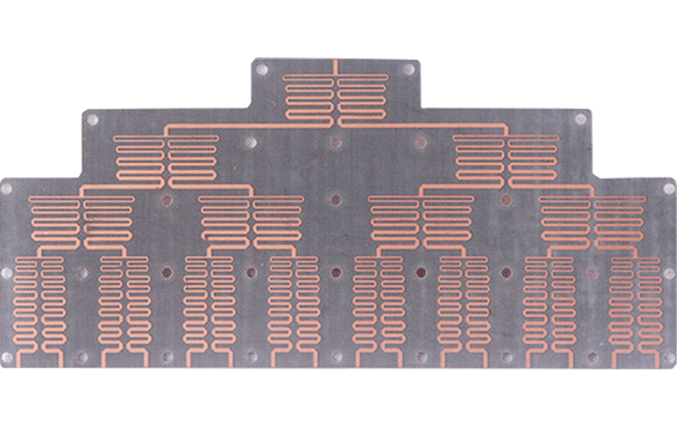
Three Tiers of "Communication Equipment"
The word covers products whose requirements differ by an order of magnitude, and 4003C does not serve all three equally. It is worth separating them before quoting any parameter:
- Infrastructure — base station antenna arrays, remote radio units, microwave backhaul radios, satellite ground terminals. Long RF runs, tight phase requirements, outdoor thermal cycling.
- Short-range radios — Wi-Fi access points, IoT gateways, RFID readers. Short traces, cost-sensitive, and very often adequately served by FR-4.
- Consumer terminals — phones, wearables. High layer counts, HDI, antenna-in-package; laminate choice is driven by the antenna substrate, not by the radio board.
4003C’s real territory is the first tier and the upper half of the second. Presenting it as the material for “communications” in general is how a specification ends up paying 3–5 times FR-4 cost for a link that never needed it.
The Data Sheet Numbers That Actually Decide
Values below are the RO4000 series data sheet figures for RO4003C. The two that matter most in communication design are not the two that get quoted most: Dk tolerance decides filter centring and impedance, and TCDk decides phase drift over temperature. Df decides how far you can go.
| Property | RO4003C | Why it matters in a radio |
|---|---|---|
| Dk, process | 3.38 ±0.05 @ 10 GHz | ±0.05 on 3.38 is ±1.5 %, which moves a 50 Ω line by ±0.74 % and a resonant filter by the same ±0.74 % in frequency |
| Dk, design | 3.55 (8–40 GHz) | Use this for modelling broadband structures; using 3.38 as a design value makes lines 2.5 % short |
| Df | 0.0027 @ 10 GHz, 0.0021 @ 2.5 GHz | Loss rises with frequency on the same sheet — quoting 0.0027 for a 2.4 GHz design overstates loss by about 29 % |
| TCDk | +40 ppm/°C (−50 to 150 °C) | 0.5 % Dk change over 125 K → 5.5° phase drift per 100 mm at 10 GHz, 15° at 28 GHz |
| CTE | X 11 / Y 14 / Z 46 ppm/°C | X/Y below copper (17) is a registration advantage; Z at 2.7× copper is a plated-hole strain item |
| Tg / Td | >280 °C / 425 °C | Survives lead-free reflow and repeated rework without expansion stepping at process temperature |
| Thermal conductivity | 0.71 W/(m·K) | 0.254 mm of dielectric = 3.58 K·cm²/W; at 10 W/cm² that is a 35.8 K rise across the laminate alone |
| Moisture absorption | 0.06 % | Low enough that humidity is not a Dk problem; still bake before reflow per the MSL of the assembly |
| Peel strength | 1.05 N/mm (6 pli), 1 oz ED after solder float | Higher than 4350B’s 0.88 N/mm, which is why fine-line and multiple reflow routes favour 4003C |
| Flammability | N/A — no UL 94 grade | The single most common compliance surprise on this material; see the section below |
Where 4003C Sits in the Line-Up
Four laminates cover most communication work. The comparison that decides a project is not “which is best” but “which constraint binds first”:
| Laminate | Dk | Df | k, W/(m·K) | UL 94 | Binds first |
|---|---|---|---|---|---|
| FR-4 | 4.2–4.6 | 0.018–0.025 | 0.25–0.35 | V-0 | Dielectric loss above roughly 3 GHz; Dk tolerance ±0.2 or worse |
| RO4003C | 3.38 ±0.05 | 0.0027 | 0.71 | none | Flammability spec, or copper loss on thin cores |
| RO4350B | 3.48 ±0.05 | 0.0037 | 0.69 | V-0 | Loss — about 40 % more dielectric loss than 4003C for the same geometry |
| RO3003 / 5880 / TLY-5 | 2.20–3.00 | 0.0009–0.0010 | 0.20–0.50 | V-0 (5880) | Price and process — PTFE needs dedicated bonding and hole activation |
The cost ladder follows the same order: roughly 1× for FR-4, 3–5× for the RO4000 family by panel area, and 10–20× for PTFE grades once the extra process steps are counted. The reason 4003C dominates infrastructure radios is not that it is the lowest-loss material available — it is the lowest-loss material that a normal FR-4 shop can run without changing its hole-plating line.
The head-to-head with 4350B is worth its own reading, because the two are frequently substituted for each other on the assumption that they are interchangeable; they are not, and the difference is flammability as much as loss. It is covered in the 4350B versus 4003C comparison.
Band by Band: What 100 mm Costs
This is the table to design against. Assumptions: 50 Ω microstrip, 1 oz copper, 0.508 mm core, εeff 2.67, loss split into dielectric (scales with Df) and conductor (scales with √f). Df above 10 GHz is extrapolated from the data sheet trend and should be replaced by measured data for a production release.
| Band | Dielectric loss, dB/100 mm | Conductor loss, dB/100 mm | Total, dB/100 mm | Length for a 20 dB budget |
|---|---|---|---|---|
| 2.5 GHz | 0.09 | 0.39 | 0.48 | 4.2 m |
| 3.5 GHz (5G sub-6) | 0.13 | 0.46 | 0.59 | 3.4 m |
| 6 GHz (Wi-Fi 6E) | 0.24 | 0.61 | 0.85 | 2.4 m |
| 10 GHz | 0.45 | 0.79 | 1.24 | 1.6 m |
| 24 GHz | 1.21 | 1.22 | 2.42 | 0.83 m |
| 28 GHz | 1.41 | 1.31 | 2.72 | 0.73 m |
| 39 GHz | 2.15 | 1.55 | 3.71 | 0.54 m |
Two conclusions fall out of it. First, below about 6 GHz the conductor term dominates — more than 70 % of the loss at 2.5 GHz — so buying a lower-Df laminate at those frequencies barely moves the link. Second, above 10 GHz the dielectric term takes over and grows faster than the conductor term, which is where the material choice genuinely decides feasibility.
The conductor term is also a geometry lever. A thicker core gives a wider 50 Ω line for the same impedance, and a wider line spreads the same current over more copper: at 10 GHz, the same 50 Ω line runs about 0.24 dB/in on a 0.203 mm core but roughly 0.10 dB/in on a 0.813 mm core, before fringing corrections. Dielectric loss per millimetre does not change — so a thicker laminate can be the cheaper way to cut total insertion loss, at the cost of board thickness and via stub length.
Base Stations, Antenna Arrays and Radio Units
Three different jobs sit inside one radio unit, and 4003C is asked to do all three:
- Array feed networks — the requirement is amplitude and phase consistency across channels, not raw loss. Dk tolerance ±0.05 and thickness tolerance ±10 % (which costs about ±6 % impedance) dominate; on a corporate feed with unequal path lengths, Dk variation between laminates shifts the beam.
- Filters — coupling coefficients scale with Dk, so the same ±1.5 % Dk tolerance shifts centre frequency by ±0.74 %. A narrowband filter with 1 % bandwidth is therefore already at the edge of the material tolerance; this is where a tight Dk window matters more than a low Df.
- Power amplifiers — the laminate carries the heat out of the transistor, and 4003C’s 0.71 W/(m·K) is respectable for a thermoset but still an insulator. The vertical thermal resistance of the dielectric is the number that decides the junction temperature, not the copper weight around it.
| Material | k, W/(m·K) | R″ of a 0.254 mm layer | Rise at 10 W/cm² |
|---|---|---|---|
| RO4003C | 0.71 | 3.58 K·cm²/W | 35.8 K |
| RO4350B | 0.69 | 3.68 K·cm²/W | 36.8 K |
| FR-4 | 0.30 | 8.47 K·cm²/W | 84.7 K |
| RT/duroid 5880 | 0.20 | 12.7 K·cm²/W | 127 K |
The 4003C advantage over FR-4 here is real and under-quoted: 2.4× the thermal conductivity means less than half the temperature rise across the same dielectric thickness. But it is not a heat-spreading feature — it shortens the vertical path only. Lateral spreading still has to come from copper planes and thermal vias, which is a stack-up decision rather than a material one (see stack-up design).
Phase drift over temperature is the other array issue. With TCDk ±40 ppm/°C, a 125 K excursion moves Dk by 0.5 %, which is 5.5° of phase on a 100 mm line at 10 GHz and 15° at 28 GHz. For a beam-steering array that is a calibration item, not a defect; for a phase-matched pair it is a tracking error, and the fix is either calibration over temperature or a material with a flatter curve.
Microwave Backhaul, 6 to 38 GHz
Point-to-point backhaul is 4003C’s home band. Radios from 6 to 38 GHz use it because the loss at those frequencies is a genuine constraint (see the band table), because the boards are small and often multilayer with a hybrid FR-4 section for control and power, and because the dielectric is a thermoset that a normal shop can drill and plate.
Thickness selection matters more than it looks. Standard cores run 0.203, 0.254, 0.305, 0.406, 0.508, 0.813 and 1.524 mm, which at Dk 3.38 correspond to 50 Ω microstrip widths of roughly 0.47, 0.59, 0.71, 0.95, 1.18, 1.89 and 3.55 mm:
| Core, mm | 50 Ω microstrip width | Consequence |
|---|---|---|
| 0.203 | 0.47 mm | Highest conductor loss, but the only option for 28–39 GHz where the λ/4 stub limit forces thin dielectric |
| 0.508 | 1.18 mm | The workhorse for 6–18 GHz: reasonable loss, manufacturable 0.2 mm vias |
| 0.813 | 1.89 mm | Lowest conductor loss per inch; used where the board is thick enough that stub resonances are not the binding issue |
| 1.524 | 3.55 mm | Wide lines at low impedance spread; only for low-frequency, high-power or mechanical-stiffness reasons |
Above roughly 20 GHz the laminate stops being the limiting factor and the copper finish starts to be. Electroless nickel at 3–6 µm sits inside the skin depth at those frequencies (0.65 µm for copper at 10 GHz, 1.33 µm for nickel), so the current runs in a poorer conductor. If the loss budget is tight above 20 GHz, specify immersion silver or OSP rather than ENIG, and treat the finish as an electrical decision.
Wi-Fi, IoT and RFID: Where FR-4 Is the Right Answer
This is the part of the original article that needed the most correction, because it lists WLAN, RFID and IoT gateways as 4003C applications without checking the numbers. At 2.4 GHz, 4003C spends 0.48 dB per 100 mm and FR-4 spends about 1.3 dB — on a 30 mm trace, the difference is 0.25 dB. No Wi-Fi link budget notices that.
So when does a short-range radio genuinely need 4003C? Four cases:
- The filter or coupler is the product. A printed filter with 2 % bandwidth needs Dk tolerance an order tighter than FR-4 delivers, regardless of frequency.
- The antenna is printed on the board and phase matters. Arrays and beamforming front ends at 5–6 GHz, where FR-4’s Dk varies by batch as well as by position.
- Loss is a thermal problem. A high-duty-cycle PA where 1 dB of trace loss becomes a heatsink requirement.
- The board must also carry a millimetre-wave section. One laminate for the whole stack is simpler than a hybrid, and at 24 GHz+ the FR-4 section would not work.
Outside those, FR-4 with a careful stack-up is the honest recommendation — and telling a customer that is more useful than upselling a laminate whose advantage disappears at 30 mm of trace length. The general trade-off between the two families is worked through in high-frequency PCB versus standard PCB.
RFID deserves one specific note: passive UHF tags at 860–960 MHz and HF tags at 13.56 MHz are antenna-design problems, and the tag substrate is usually PET or paper in a printed process, not a laminate at all. A reader’s RF board is a different question from the tag.
Satellite and Ground Terminals: What 4003C Covers
Ground terminals, block up-converters and low-noise blocks are legitimate 4003C territory at Ku and Ka band, and the original article is right that the material works there. What it overstated is the reason, and it left out the qualifier that a satellite programme will ask for first.
The omitted qualifier is outgassing. Space hardware is qualified against ASTM E595, with total mass loss and collected volatile condensable material limits typically stated by the programme; PTFE grades such as RT/duroid 5880 and Taconic TLY-5 carry published outgassing figures, RO4003C is not specified for it on the data sheet. If the board flies, ask for the data rather than assume the 0.06 % moisture figure covers it — it does not, because outgassing is about volatiles leaving, not water going in.
The other honest limit is phase over temperature. TCDk +40 ppm/°C is good for a thermoset but it is not flat: on a long feed chain in a terminal that swings 100 K between sun and shade, that is measurable phase movement. Where phase stability over temperature dominates, the PTFE family with much lower and often negative TCDk is chosen — see the 5880 laminate parameters for the comparison basis, and note that the trade is process complexity, not just price.
The Compliance Gap: 4003C Has No UL 94 Grade
On the RO4000 data sheet, the flammability row for RO4003C reads “N/A”, while both RO4350B and RO4835 carry V-0. This is not a printing error and it is not a small print item: it decides material choice on a large share of communication projects, because telecom operators and enterprise customers routinely require V-0 at bare-board level even when the end product would pass without it.
| Situation | What to do |
|---|---|
| Customer spec says “UL 94 V-0 laminate” | 4003C cannot satisfy it. Use RO4350B or RO4835 and accept roughly 40 % more dielectric loss, or negotiate the requirement in writing |
| No flammability requirement stated | 4003C is fine and is the lower-loss choice; state the absence of a grade explicitly in the qualification record so it does not surface later |
| Prototype now, certification later | Decide before layout, not after. Switching laminate after impedance is tuned costs a full re-spin of every controlled line |
The mechanism behind the gap is worth knowing, because it explains why you cannot buy your way out of it within the same family: flame retardancy in this chemistry comes from halogenated or phosphorus-containing groups, and those groups raise Df. Low loss and V-0 are pulling in opposite directions, and 4003C sits on the low-loss side of that line.
Process Reality: FR-4-Like, With Three Differences
4003C is a hydrocarbon/ceramic thermoset, not PTFE, so it runs on a standard FR-4 line — but three differences change the process window and should appear in the fabrication note:
- Lamination at 190–200 °C rather than the 170–190 °C of standard FR-4, with a bondply such as RO4450B/F rather than generic FR-4 prepreg at the RF interface. The bondply has a higher Df than the core, so its thickness has to be included in the impedance model — omitting it is one of the most common causes of a board arriving 10–20 % high in impedance.
- No sodium-naphthalene or plasma activation for plated holes. This is the operational advantage over PTFE: the desmear and plating line does not change, which is why the cost multiplier stays at 3–5× instead of 10–20×.
- PTH strain from Z-axis expansion. 46 ppm/°C is 2.7× copper. It is manageable — far easier than PTFE’s 217–237 — but it still sets a rule: keep aspect ratio within the shop’s qualified range and specify a plating elongation that accommodates the expansion over the reflow excursion.
The design-side sequence that produces a manufacturable 4003C board is the same seven-stage flow used for any high-frequency design, and the impedance budget is where most of the risk sits — see design steps and key considerations. For the 4003C-specific fabrication walkthrough, including thickness and copper options, the 4003C laminate guide is the companion piece to this one.
Five Claims From the Original Article That Do Not Hold
| Claim | What is actually true |
|---|---|
| “The material’s low loss and good EMC reduce interference” | A dielectric does not shield. EMC performance comes from continuous reference planes, edge plating, filtering and enclosure design. The laminate contributes indirectly: Dk tolerance shifts filter centring, and Df sets loss — neither is shielding |
| “CTE 46 is close to FR-4, so the board will not delaminate or warp” | CTE does not prevent delamination; bonding does. 46 ppm/°C is 2.7× copper, so the real consequence is strain in plated holes and, on asymmetric stacks, warp |
| “Thermal conductivity 0.5 W/m·K” | The data sheet value is 0.71 W/(m·K). The error matters, because it is the parameter used to justify a heatsink decision |
| “Excellent for satellite links above 10 GHz” | It works at Ku/Ka band, but there is no published ASTM E595 outgassing qualification, and TCDk +40 ppm/°C produces measurable phase drift on long feeds |
| “FR-4 process compatibility lowers cost for mass production” | Compatibility lowers the process premium, not the material price: expect 3–5× FR-4 by area. And the UL 94 gap can make the material unusable regardless of cost |
Conclusion
4003C earns its place in communication equipment on three counts: a loss level that keeps 100 mm of trace under 1.3 dB up to 10 GHz, a Dk tolerance tight enough to centre filters, and an FR-4 process window that avoids the PTFE premium. It loses on three others: flammability (no UL 94 grade), thermal spread (0.71 W/(m·K) is 2.4× FR-4 but still an insulator), and any link long enough that the 28–39 GHz numbers matter.
Design against the band table rather than the headline Df, state the UL question before layout, and put the bondply in the impedance model. Those three habits prevent most of the failures attributed to this material.
The same logic applied to a different sector — medical devices, where the binding constraint is qualification rather than loss — is in the medical device companion article, and the cross-industry material map is in applications of Rogers high-frequency PCB by industry.
XCE PCB fabricates RO4003C from 2 to 72 layers with impedance held to ±10 %, panel sizes to 600×1200 mm, 80+ engineers and 10,000+ documented builds since 2009 — samples in as fast as 24 hours.
Frequently Asked Questions
Is Rogers 4003C suitable for 5G base stations?
Does Rogers 4003C have a UL 94 rating?
What is the difference between 3.38 and 3.55 for RO4003C?
How much loss does Rogers 4003C add at 10 GHz?
Is Rogers 4003C good for Wi-Fi and IoT boards?
Can Rogers 4003C be used in satellites?
Need 4003C Boards With a Measured Loss Budget?
Send us your Gerber files and requirements for a manufacturability review and a tailored quotation.
sales1@xcepcb.com
+86 180 3818 8537