
RT/duroid 6002 is usually sold with a list of virtues — low loss, stable Dk, copper-matched expansion, low outgassing — and almost never with the arithmetic that shows what those virtues cost. Rogers RT6002 is Dk 2.94 and Df 0.0012 at 10 GHz, with +12 ppm/°C on the dielectric constant and 16/16/24 ppm/°C on expansion. Those four numbers pull in different directions, and each one is paid for by another.
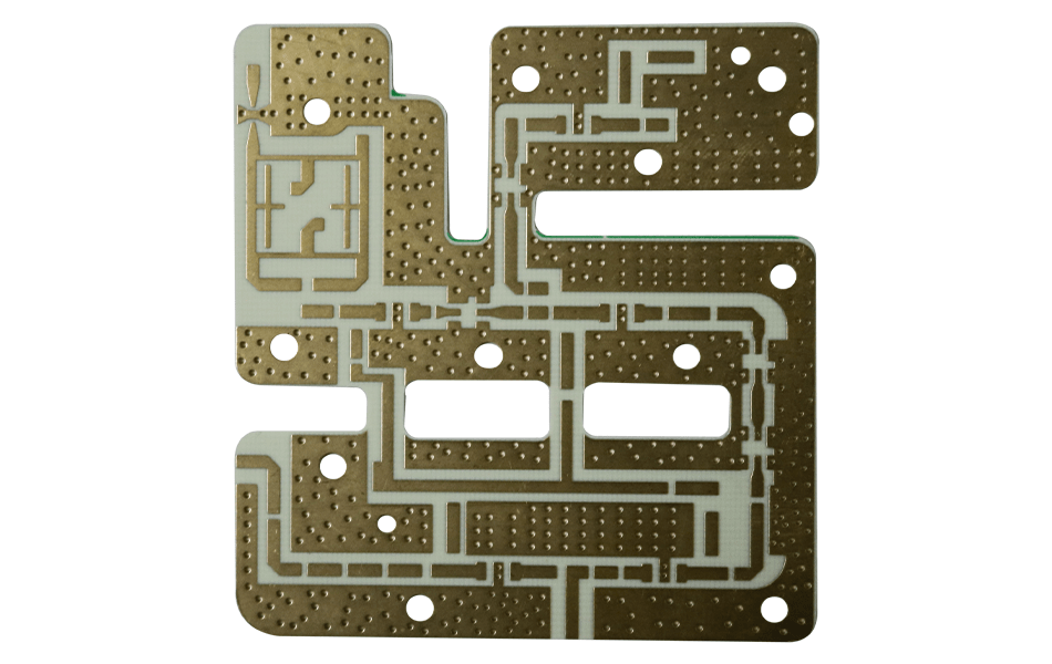
What RT/duroid 6002 Is, and Why It Exists Between Two Better-Known Materials
RT/duroid 6002 is a PTFE laminate with micro glass fibre reinforcement. It sits between two materials that get far more attention: the RT/duroid 5880 at Dk 2.20 / Df 0.0009, which is the lowest-loss choice, and RO3003 at Dk 3.00 / Df 0.0010, which is the ceramic-filled grade with no glass at all.
On a specification sheet 6002 looks like a compromise between the two, and in one sense it is: it loses to 5880 on dissipation factor and loses to 3003 on Df as well. What it does not lose on is the pair of numbers that decide whether a multilayer microwave board can be built at all — 16/16 ppm/°C in-plane expansion against copper’s 17, and 24 ppm/°C in Z. Those are the numbers the rest of this article is about, because they are the reason the material has stayed in phased-array and radar programmes for decades while better-loss materials have come and gone.
Read against the rest of the RT/duroid family, 6002 is the dimensional-stability branch rather than the loss branch. That distinction decides which of its parameters you are allowed to complain about.
The Published Parameter Set
The table below is the current Rogers data sheet, not a summary of it. Every later section derives from these rows, and the tolerances matter as much as the typical values — a typical number tells you what the material can do, a tolerance tells you what you can hold in production.
| Property | Value | Condition / method |
|---|---|---|
| Dielectric constant, process | 2.94 ± 0.04 | 10 GHz, 23 °C, IPC-TM-650 2.5.5.5 |
| Dielectric constant, design | 2.94 | Same value as process — no design offset |
| Dissipation factor | 0.0012 | 10 GHz, 23 °C |
| Thermal coefficient of Dk | +12 ppm/°C | 10 GHz, −50 to +150 °C |
| CTE, X / Y / Z | 16 / 16 / 24 ppm/°C | −55 to +288 °C, ASTM D3386 |
| Thermal conductivity | 0.60 W/m·K | 50 °C, ASTM D5470 |
| Water absorption | 0.02 % | D48/50 immersion |
| Peel strength | 8.9 lb/in (1.6 N/mm) | 1 oz (35 µm) ED foil |
| Density | 2.1 g/cm³ | — |
| Decomposition temperature | 500 °C | TGA; lead-free compatible |
| Flammability | UL 94 V-0 | Listed grade |
Two features of this table are worth flagging before the arithmetic starts. The design Dk equals the process Dk, which is unusual — the RO4000 family carries a 0.1–0.2 offset between the two, and designs built on the wrong one of those numbers land 2–3 % off in impedance. And the peel strength of 1.6 N/mm for 1 oz ED foil is high for a PTFE composite, which is a fabrication advantage that never appears in a marketing summary.
Dk 2.94: Eleven Percent Shorter Wavelength, Paid for in Line Width
Calling 2.94 a “low” dielectric constant is true only relative to FR-4 at 4.3. Against 5880 it is 34 % higher, and the consequences run in two directions at once.
The useful consequence is electrical length. A microstrip on 6002 has an effective permittivity of about 2.38 at 50 Ω, so a guided wavelength at 10 GHz is 19.4 mm against 21.9 mm on 5880. The same physical route is 11 % more electrical degrees, or conversely a filter or a corporate feed occupies 11 % less board area for the same design. On a phased-array panel where element pitch fixes the outline, those degrees are what lets the feed network fit.
| Material | Dk | W/h for 50 Ω microstrip | εeff | Guided wavelength at 10 GHz | Width on 0.254 mm core |
|---|---|---|---|---|---|
| RT/duroid 5880 | 2.20 | 3.11 | 1.87 | 21.9 mm | 0.79 mm |
| RT/duroid 6002 | 2.94 | 2.56 | 2.38 | 19.4 mm | 0.65 mm |
| RO3003 | 3.00 | 2.54 | 2.42 | 19.3 mm | 0.65 mm |
| RO4003C | 3.38 | 2.33 | 2.67 | 18.4 mm | 0.59 mm |
| RO4350B | 3.48 | 2.27 | 2.72 | 18.2 mm | 0.58 mm |
The cost is on the right-hand side. For a fixed dielectric thickness, higher Dk means a narrower 50 Ω trace, and a narrower trace means every etch tolerance becomes a larger fraction of the width. On a 0.254 mm core the 6002 line is 0.65 mm wide, so ±25 µm of etch is 3.8 % of the width — about ±2 % of impedance. On a 5880 build at 0.79 mm the same tolerance is 3.2 %. The gap is small here, but it grows on thin cores: at 0.127 mm the 6002 line is 0.33 mm wide and the same ±25 µm is 7.6 % of the width, which is ±3.8 % of impedance before anything else is counted.
Thickness tolerance dominates that budget regardless of material. A ±10 % core variation moves a 50 Ω microstrip from 50.0 to 46.8 or 53.0 Ω, and Dk’s own ±0.04 (1.36 %) contributes about ±0.7 %. That is why a 6002 order should state the finished dielectric height and the impedance target together, not the laminate part number alone.
Df 0.0012: A 33 % Gap That Mostly Does Not Matter at 10 GHz
The dielectric part of insertion loss follows a simple proportionality, αd ≈ 2.6 · fGHz · √Dk · Df in dB/in. Run it and 6002 lands 33 % above 5880 — a number that sounds decisive and usually is not, because at 10 GHz on a 0.254 mm core the copper contributes three to four times what the dielectric does.
| Material | Df | Dielectric loss 10 GHz | 28 GHz | 77 GHz | Total microstrip, 10 GHz, 0.254 mm, 1 oz |
|---|---|---|---|---|---|
| FR-4 | 0.020 | 1.09 dB/in | 3.05 dB/in | 8.4 dB/in | 1.28 dB/in |
| RO4350B | 0.0037 | 0.18 dB/in | 0.50 dB/in | 1.38 dB/in | 0.38 dB/in |
| RO4003C | 0.0027 | 0.13 dB/in | 0.36 dB/in | 1.00 dB/in | 0.32 dB/in |
| RT/duroid 6002 | 0.0012 | 0.054 dB/in | 0.150 dB/in | 0.41 dB/in | 0.24 dB/in |
| RT/duroid 5880 | 0.0009 | 0.035 dB/in | 0.097 dB/in | 0.27 dB/in | 0.22 dB/in |
Read the last column: 6002 and 5880 differ by 0.02 dB/in at 10 GHz, about 9 %, because the copper term is common to both and dominates. That is why replacing 5880 with 6002 to gain dimensional stability usually costs almost nothing in a 10 GHz design, and why the reverse swap rarely delivers the improvement people expect.
At millimetre wave the balance shifts. Per 100 mm the dielectric term is 1.62 dB on 6002 against 1.05 dB on 5880 at 77 GHz — a 0.57 dB difference that is now worth arguing about, especially in a receive chain where it sits ahead of the LNA. Copper roughness compounds it: Rogers’ own 77 GHz comparison on 5 mil 6002 shows rolled copper at 0.3 µm RMS beating ED copper at 1.8 µm by a margin larger than the dielectric gap between these two laminates. Above 30 GHz, if loss is the governing requirement, the material choice should be 5880 and the copper choice should be rolled — not 6002 with ordinary foil.
TCDk +12: Phase Drift Expressed in Degrees
+12 ppm/°C is quoted so often as a virtue that its magnitude is rarely converted into anything a system engineer can use. The conversion is two steps: temperature change times TCDk gives a fractional Dk change; half of that, because effective permittivity moves roughly half as much as Dk, gives a fractional electrical-length change; multiply by the phase accumulated over the line and you have degrees.
Over a 200 °C excursion, 12 ppm/°C is a 0.24 % Dk change, which is 0.12 % of phase — 2.2 degrees on a 100 mm line at 10 GHz, and 6.2 degrees at 28 GHz.
| Material | TCDk | Dk change over 200 °C | Phase drift, 10 GHz / 100 mm | Phase drift, 28 GHz / 100 mm |
|---|---|---|---|---|
| RO3003 | −3 ppm/°C | 0.06 % | 0.6° | 1.6° |
| RT/duroid 6002 | +12 ppm/°C | 0.24 % | 2.2° | 6.2° |
| RO4003C | +40 ppm/°C | 0.80 % | 7.9° | 22° |
| RO4350B | +50 ppm/°C | 1.00 % | 9.9° | 28° |
| RT/duroid 5880 | −125 ppm/°C | 2.50 % | 21° | 59° |
The spread in this table is nearly two orders of magnitude, and the sign matters as much as the size: 5880’s Dk falls as it warms while 6002’s rises, so a phase shifter trimmed on one cannot be trimmed the same way on the other. For a delay-line or a filter whose passband edge is set by electrical length, 2.2 degrees over the full military range is a design that needs no compensation network; 21 degrees is a design that needs a heater or a calibration table. That, more than the loss figure, is why 6002 keeps appearing in delay lines and 5880 does not.
Z-CTE 24: The Via Strain Arithmetic
The Z-axis coefficient is the parameter that decides plated-hole life, and the arithmetic is a multiplication: expansion coefficient, times temperature excursion, times board thickness. For a 1.6 mm board through a lead-free reflow of 215 K, 24 ppm/°C gives 8.3 µm of dielectric expansion. The same sum on 5880 gives 81 µm.
| Material | Z-CTE | Expansion of 1.6 mm across 215 K | Tensile strain on a plated barrel |
|---|---|---|---|
| RT/duroid 6002 | 24 ppm/°C | 8.3 µm | 0.52 % |
| RO3003 | 25 ppm/°C | 8.6 µm | 0.54 % |
| RO4350B | 32 ppm/°C | 11.0 µm | 0.69 % |
| RT/duroid 6010.2LM | 47 ppm/°C | 16.2 µm | 1.01 % |
| Taconic TLY-5 | 217 ppm/°C | 74.6 µm | 4.66 % |
| RT/duroid 5880 | 237 ppm/°C | 81.5 µm | 5.09 % |
Electroplated copper ruptures somewhere around 6–10 % elongation, so a single excursion is survivable on every material in this table. The reason 5880 boards still fail is cumulative: the barrel is a thin film in a state of constant tension, and every reflow, rework cycle and thermal shock spends some of its remaining ductility. 0.52 % per cycle against 5.09 % is a factor of ten in fatigue life, which is the difference between a board that survives three assembly reflows and one that survives a screening campaign.
Two rules follow. Plating must be high-ductility, with elongation at or above 20 % as a purchase condition rather than a hope. And the aspect ratio should stay at or below 6:1, because the strain is distributed over the barrel length but the fatigue damage concentrates at the surface-to-barrel transition. Where the thermal path matters more than the electrical one, 6035HTC trades a 19/19/39 CTE and 1.44 W/m·K for a lower-Dk alternative; 6002 at 0.60 W/m·K sits in the middle and needs thermal vias to release heat from a dissipative component.
X/Y 16 Against Copper 17: The Parameter That Actually Sells the Material
In-plane expansion is where 6002 is genuinely unusual, and where its marketing claim survives measurement. Copper expands at 17 ppm/°C; 6002 expands at 16. The 1 ppm difference is the smallest mismatch available in any commercial microwave laminate, and it is what makes sequential lamination and blind-via registration predictable.
| Material | X / Y CTE | Mismatch to copper (17) | Differential movement, 600 mm panel, 200 K | Registration consequence |
|---|---|---|---|---|
| RT/duroid 6002 | 16 / 16 | 1 ppm/°C | 0.12 mm | Predictable, single scale factor |
| RO3003 | 17 / 16 | 0–1 ppm/°C | 0.12 mm | Same class |
| RO4350B | 10 / 12 | 5–7 ppm/°C | 0.84 mm | Laminate shrinks less than copper; pad-side shift |
| RT/duroid 5880 | 31 / 48 | 14–31 ppm/°C | 1.68 mm | Anisotropic; X and Y need different compensation |
The right-hand column is the one that changes a process. On a glass-free PTFE the panel grows differently in X and Y, so a single CAM scale factor cannot serve both axes and fabricators fall back on per-axis compensation, test coupons, or the costly practice of etching and re-etching with measured offsets. On 6002 the panel moves almost exactly as the copper does, so one scale factor holds across a 600 mm panel and 0.12 mm of residual is a number you can put in a stack-up note instead of discovering at X-ray.
That is also the honest version of the claim that 6002 removes the need for dimensional compensation. It does not remove it — 0.12 mm at 600 mm is still 20 % of a ±0.05 mm registration budget — but it makes the compensation a constant rather than a per-lot measurement.
6002 Against RO3003: Nearly Identical Numbers, Different Construction
Put the two side by side and the surprise is how little separates them. Dk 2.94 against 3.00, Df 0.0012 against 0.0010, Z-CTE 24 against 25, in-plane 16/16 against 17/16. A buyer could reasonably ask why both exist.
| Property | RT/duroid 6002 | RO3003 | What the difference decides |
|---|---|---|---|
| Construction | PTFE with micro glass fibre | Ceramic-filled PTFE, no glass | Mechanical toughness vs Dk uniformity at fine features |
| Dk / Df | 2.94 / 0.0012 | 3.00 / 0.0010 | 3003 is 17 % lower in dielectric loss; measured total difference at 10 GHz is under 0.01 dB/in |
| TCDk | +12 ppm/°C | −3 ppm/°C | 3003 for phase-critical delay lines |
| Thermal conductivity | 0.60 W/m·K | 0.50 W/m·K | 6002 spreads heat 20 % better |
| Peel strength | 1.6 N/mm | Higher with glass reinforcement | Rework and connector retention |
| Dielectric strength | Reported per data sheet | Reported per data sheet | Neither is a high-voltage material |
The practical split is this: choose 6002 when the board is a mechanical object under thermal load — large panels, thick multilayer, connectors that get torqued, assemblies that see repeated reflow — and choose 3003 when the circuit is a phase reference and the dielectric must not move with temperature at all. Between them, 6002’s lower cost of ownership comes from yield rather than from electrical margin.
Where 6002 Beats 5880, and Where It Does Not
Most selection arguments in this family reduce to one question: can the design tolerate 33 % more dissipation factor in exchange for ten times less Z-axis expansion and six times less phase drift.
| Requirement | Better choice | Reasoning |
|---|---|---|
| Long run at 30–77 GHz, receive side | 5880 | 0.57 dB per 100 mm difference at 77 GHz sits ahead of the LNA |
| Delay line or filter over −55 to +125 °C | 6002 (or 3003) | 2.2° against 21° of phase drift per 100 mm at 10 GHz |
| Eight-layer board with blind vias | 6002 | 1 ppm in-plane mismatch; one CAM scale factor |
| Thick assembly, three reflows | 6002 | 8.3 µm against 81 µm of Z expansion at 1.6 mm |
| Radome-facing antenna, cost sensitive | RO4003C / RO4350B | At 10 GHz the loss penalty is modest and the process is FR-4 compatible |
The third row is where the material earns its price. On a design with two lamination cycles, the registration error from Z expansion is not the binding constraint; it is the in-plane growth that puts layer 2 pads under layer 5 vias. That failure mode has nothing to do with Df, and no amount of low-loss material will fix it. Comparisons of 4350B and 4003C on the same axis are set out in the 4350B and 4003C selection guide.
Thickness Options and the 50 Ohm Line They Impose
6002 is supplied in standard cores from 0.127 mm to 3.175 mm; thicker builds are made by lamination rather than by ordering a slab. Because W/h is fixed at 2.56, every thickness step fixes the line width, and the pattern of those widths explains why most 6002 designs cluster at the thin end.
| Core thickness | 50 Ω microstrip width | ±25 µm as % of width | Impedance effect of that etch tolerance | Typical use |
|---|---|---|---|---|
| 0.127 mm | 0.33 mm | 7.6 % | ±3.8 % | mmWave antenna layers; tolerance-dominated |
| 0.254 mm | 0.65 mm | 3.8 % | ±1.9 % | The default microwave stack |
| 0.508 mm | 1.30 mm | 1.9 % | ±1.0 % | Filters, couplers with relaxed density |
| 1.016 mm | 2.60 mm | 1.0 % | ±0.5 % | High-power feeds; wide lines needed for current |
| 1.524 mm | 3.90 mm | 0.6 % | ±0.3 % | Rigid antenna substrates, mechanical flatness |
Two practical notes. A 3.90 mm trace on 1.524 mm laminate is wider than many corporate-feed geometries allow, so thick 6002 tends to appear on antenna faces rather than in distribution networks. And on thin cores the width becomes small enough that the mask resolution and the etch compensation, not the laminate, decide the final impedance — which is a conversation with the fabricator, not with Rogers.
Fabrication: What Actually Changes on a PTFE/Glass Build
6002 processes like PTFE, not like FR-4, and the differences are concentrated in five steps.
Hole wall preparation. Permanganate desmear does not attack PTFE, so the standard FR-4 sequence leaves an unmodified wall that nothing will plate to. Sodium naphthalenide or a plasma cycle is mandatory before electroless copper; skipping it produces holes that pass electrical test and fail thermal cycling.
Drilling. PTFE is soft and abrasive filler is not, so the drill sharpness matters more than the speed. Entries and exits should be backed, stacks kept to three or fewer, and the aspect ratio held to 6:1 — the same limit that the Z-CTE arithmetic in section 6 produces.
Lamination. 6002 can be direct-bonded without adhesive, which is one of its quieter advantages for multilayer work; where a bondply is used, 3001 film or a low-flow prepreg is the route, at 290–315 °C for fusion bonding or 180–190 °C for the low-flow film. The 260–300 °C window cannot be shared with an FR-4 co-cure: mixed constructions have to be sequenced, as described in the multilayer PTFE processing notes.
Stress relief after etching. RT/duroid laminates are supplied with residual stress from their own manufacture; after inner-layer etching, a bake is required before lamination to prevent the pattern moving during the press. Skipping the bake shows up as layer-to-layer shift that looks like a registration problem and is not.
Surface finish. HASL is not an option at 250–260 °C on a material whose Z expansion is 24 ppm/°C and whose dielectric cold-flows under pressure. ENIG, immersion silver and OSP are the RF set; above 20 GHz the 3–6 µm nickel in ENIG becomes the dominant conductor, and immersion silver or a nickel-free finish is the better answer. Cold flow also has to be designed for: a 4 % compression of the dielectric moves a 50 Ω line to 48.8 Ω, and the change does not come back when the clamp is released.
The Claims in Circulation, Audited
Six statements about 6002 appear repeatedly in supplier articles. Four are defensible with a qualifier, one needs a test report, and one is simply wrong about our own capability.
| Claim | Verdict |
|---|---|
| 6002 is a low-Dk laminate | Only against FR-4. At 2.94 it is 34 % above 5880 and 2 % below 3003; describing it as low invites comparisons it loses |
| Dk is stable from −55 to +150 °C | Supported: +12 ppm/°C is the published figure over −50 to +150 °C, and it is 10× smaller than 5880’s. Quote the number, not the adjective |
| 5000 thermal cycles at −55/+150 °C with no via failures | No public source. The arithmetic supports long life (8.3 µm expansion at 1.6 mm), but a cycle count belongs in a qualification report you have read, not in a purchase specification |
| In-plane CTE matched to copper removes the need for dimensional compensation | Directionally right, quantitatively overstated: 1 ppm mismatch still leaves 0.12 mm across a 600 mm panel over 200 K. It makes the scale factor constant, not zero |
| Low outgassing makes it suitable for space | The PTFE chemistry supports the claim, but ASTM E595 TML and CVCM values must come from a lot-specific report. Do not let a marketing sentence stand in for the data |
| Suitable for 2–64 layer boards | A capability statement that belongs to the fabricator, not the laminate. Our own window is 2–72 layers, 600×1200 mm, impedance ±10 % — and the practical limit on a PTFE build is set by aspect ratio and press cycles, not by layer count |
What to Put on a 6002 Order
Six items turn the data sheet into a specification that can be inspected:
1. Laminate and thickness per layer, with the finished dielectric height rather than the nominal core, because 0.254 mm core plus bondply is not 0.254 mm of dielectric. 2. Impedance target per layer with coupon geometry — on 6002 the etch sensitivity is ±1.9 % on a 0.65 mm line, so a ±10 % window is achievable while ±5 % needs the thicker cores. 3. Copper type and weight; specify rolled copper above 30 GHz and state the roughness you are buying, since 0.3 µm against 1.8 µm MSE moves total loss more than the choice between 6002 and 5880. 4. PTH process — sodium naphthalenide or plasma, stated, with the plating elongation requirement of ≥ 20 %. 5. Surface finish, with the nickel-bearing option explicitly excluded above 20 GHz. 6. Post-etch bake and press sequence for any build with two or more lamination cycles.
With those six, a 6002 order is a set of measurable conditions. Without them, it is a part number that two fabricators will interpret differently — and the difference will show up as a phase error nobody can trace.
Conclusion
Rogers RT6002 is not the low-loss material it is often advertised as. At Df 0.0012 it gives up 33 % to 5880 on dielectric loss, which at 10 GHz is worth only 0.02 dB/in because copper dominates, and at 77 GHz is worth 0.57 dB per 100 mm, which is real money in a receiver front end.
What it buys instead is a set of mechanical numbers that no lower-loss PTFE matches: 16/16 ppm/°C in plane against copper’s 17, 24 ppm/°C in Z, and a TCDk of +12 that converts to 2.2 degrees of phase drift per 100 mm over a 200 °C swing. On an eight-layer board with blind vias, those numbers are the difference between a process with one scale factor and a process with per-axis measurement; on a delay line, they are the difference between a calibration table and none.
XCE PCB builds 6002 and the rest of the PTFE range from 2 to 72 layers, on panels to 600×1200 mm, with impedance held to ±10 %, samples in as fast as 24 hours and inspection to IPC-A-600G and IPC-6015. Sodium-naphthalenide or plasma hole preparation, post-etch bake and coupon-based impedance verification are standard on every PTFE build, because on these materials the process is the specification. The next step in this family — how the same parameters behave when the material is chosen for application rather than for the data sheet — is covered in the RT/duroid 6002 laminate overview.
Frequently Asked Questions
What is the difference between Rogers RT6002 and RT/duroid 5880?
Is 2.94 a low dielectric constant?
How much phase drift does a +12 ppm/°C TCDk cause?
Does RT6002 really remove the need for dimensional compensation?
Why does 6002 need a bake after inner-layer etching?
Can RT6002 be used with HASL and standard FR-4 processes?
Building a Microwave Multilayer on RT/duroid 6002?
Send us your Gerber files and requirements for a manufacturability review and a tailored quotation.
sales1@xcepcb.com
+86 180 3818 8537