
A high-frequency circuit board is not defined by a frequency number. It is defined by the fact that loss and impedance have become specifications rather than consequences: the laminate is chosen for its dissipation factor, the trace width is a computed output rather than a drawing preference, and the finish is an electrical layer because at 10 GHz the current no longer runs in the copper alone. This article works from the band to the material to the loss budget to the eight process windows that decide whether the board arrives at the specified impedance — and it corrects five errors from the earlier version of this page, including the one that misclassifies an entire laminate family.
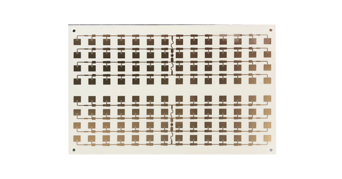
What Makes a Board “High Frequency”
The usual definition is a frequency threshold, and it is always arbitrary. One version says above 1 GHz, another says above 500 MHz, and the earlier version of this page used both in the same paragraph. The definition that survives engineering review is not a threshold but a change of regime: a board is high frequency when the loss of the interconnect matters to the system budget, or when its impedance has to be held to a tolerance.
Both conditions can be triggered at low frequencies. A 100 mm trace carrying a 500 MHz signal on FR-4 loses a fraction of a decibel, which is irrelevant to a receiver; the same trace in a phase-critical array at 500 MHz can matter because the dielectric constant moves with temperature. Conversely a short 2 GHz trace inside a module can be built on FR-4 without consequence. So the threshold is a system question, and the useful way to state it is: the frequency at which the interconnect’s contribution to the budget becomes comparable to the other terms.
What follows from that regime change is a set of practices that do not exist in commodity PCB work. The laminate is selected by dissipation factor and its tolerance. The stack is designed around a reference plane rather than around a layer count. The finish is chosen for skin depth rather than for shelf life. The coupon is designed with the artwork rather than after it. Those four practices, not a frequency number, are what distinguish the boards discussed here — and they are why the material discussion in high-frequency against standard PCB starts with loss rather than with Dk.
Where the Regime Actually Changes, Band by Band
The table converts the argument into the only form a project can use: at each band, what the interconnect costs in decibels per 100 mm on a mid-grade laminate, and what that implies for a 20 dB allocation. The numbers are for a 50 Ω microstrip on RO4003C at 0.508 mm with 1 oz copper, which is a common reference geometry.
| Frequency | Loss per 100 mm | Reach on a 20 dB allocation | What becomes the dominant term |
|---|---|---|---|
| 2.5 GHz | 0.48 dB | 4.2 m | Copper — over 70 % of the total below about 6 GHz |
| 3.5 GHz | 0.59 dB | 3.4 m | Copper, with dielectric rising |
| 6 GHz | 0.85 dB | 2.4 m | Crossover: copper and dielectric are comparable |
| 10 GHz | 1.24 dB | 1.6 m | Dielectric, and surface finish starts to matter |
| 24 GHz | 2.42 dB | 0.83 m | Dielectric, roughness, and via transitions |
| 28 GHz | 2.72 dB | 0.73 m | Dielectric; laminate grade becomes the design variable |
| 39 GHz | 3.71 dB | 0.54 m | Dielectric plus launch; connector usually dominates |
Two readings matter. The first is that below about 6 GHz the copper is the binding term, so a cheap upgrade of the foil is worth more than an expensive upgrade of the laminate. The second is that above about 24 GHz the laminate grade sets the reach, and the question stops being “which material is better” and becomes “which grade does this band need”. That is the decision the next section structures.
Four Laminate Families, Correctly Classified
The classification error that appears most often in supplier literature — and appeared in the earlier version of this page — is to place the RO3000 series among the hydrocarbon materials. It is wrong, and it matters because the two families are bonded at different temperatures and handled differently at desmear. RO3000 series laminates are ceramic-filled PTFE with no woven glass. The hydrocarbon and ceramic family is the RO4000 series, which is a thermoset processed at 190–200 °C.
| Family | Examples | Dk / Df | Chemistry | Bond temperature |
|---|---|---|---|---|
| PTFE with microglass | RT/duroid 5880, Taconic TLY-5 | 2.20 / 0.0009 | PTFE, thermoplastic, glass reinforced | 260–300 °C with FEP film |
| Ceramic-filled PTFE, no glass | RO3003, RO3006, RO3010, RO3210 | 3.00 / 0.0010 to 10.2 / 0.0022 | PTFE with ceramic filler, no woven glass | 260–300 °C, or 180–190 °C with low-flow prepreg |
| Hydrocarbon and ceramic | RO4003C, RO4350B, RO4835 | 3.38 / 0.0027 to 3.48 / 0.0037 | Thermoset, glass reinforced, FR-4 compatible | 190–200 °C |
| Modified epoxy and PPO | High-speed FR-4 variants | 3.6–4.1 / 0.008–0.012 | Thermoset, glass reinforced | 170–190 °C |
The practical consequences of the classification run in three directions. A PTFE build needs sodium-naphthalenide or plasma desmear, because permanganate does not attack it, and the smear stays in the barrel. A PTFE build is thermoplastic, so a 4 % thickness loss under press pressure is permanent and moves a 50 Ω line to 48.8 Ω. And a PTFE build cannot be co-cured with FR-4 in one cycle, so a hybrid becomes two or three presses — the arithmetic that governs both price and registration. The material baseline for each grade is catalogued in ten critical parameters for high-frequency PCBs.
One further correction belongs here. PTFE laminates are sometimes described as “typically compounded with glass cloth”. True for 5880 and TLY-5, false for the RO3000 family, which is glass-free by design so that there is no weave to create a periodic dielectric constant. The two are not interchangeable, and the absence of glass is exactly why a 3003 core behaves differently at drilling and at registration.
The Four Sections of a Radio, and Which Three Need the Material
A wireless product contains four functional sections, and the expensive laminate is only justified in three of them. Getting this wrong is the most common way a bill of materials is inflated without improving performance.
| Section | Typical frequency | Material driver | Does it need a high-frequency laminate? |
|---|---|---|---|
| Antenna and radiating structure | 0.6–79 GHz | Loss and Dk tolerance set efficiency and resonant frequency | Yes — this is where loss is least affordable |
| Feed network and filters | Same as the antenna | Loss and phase stability over temperature | Yes — phase drift here is a beam error |
| Transceiver front end | Same, at low power | Impedance control plus thermal | Yes, on the RF lines only |
| Baseband, power, control | DC to a few hundred MHz | Current capacity and solderability | No — FR-4 is the correct answer |
The last row is the one that saves money. A base station board that uses low-loss laminate under the antenna array and FR-4 under the power and control section is cheaper by 30–60 % of material cost and performs identically — provided the fabricator can run the mixed lamination cycles. The condition is not trivial: the stack has to be designed with the cure windows in mind, and the bondply between the two families is part of the transmission line and belongs in the impedance model.
Base Stations: Where the Panel Size Comes From
Massive MIMO changed the mechanical problem before it changed the electrical one. A sub-6 GHz array with 64 elements at half-wavelength spacing occupies a panel where the element pitch is fixed by physics, and the feed network has to reach every element without a connector. That is what makes 600×1200 mm panels relevant: the standard laminate sheet sets the largest board that can be built without a splice, and an antenna array is the application that needs it.
The electrical consequence is that the feed network is long, and long at 3.5 GHz on a controlled-impedance laminate is where the loss budget is spent. Using the reference geometry above, a 400 mm feed at 3.5 GHz costs about 2.4 dB on 4003C; on FR-4 the same run costs roughly 6–7 dB, and the phase drifts further with temperature. Those two numbers, not a materials argument, are why the array uses a controlled laminate.
The manufacturing consequence is registration. A 600 mm panel of PTFE or ceramic-filled PTFE expands measurably between 20 °C and the press temperature — about 0.31 mm for TLY-5 over 20 °C and 0.37 mm for 5880 — so the whole registration budget has to be managed at a controlled temperature rather than assumed. The lamination and alignment side of that problem is set out in high-frequency PCB stack-up design.
Millimetre Wave: The Finish Becomes an Electrical Layer
Above about 20 GHz three things change at once: the skin depth falls below the thickness of the finish, the copper roughness becomes comparable to the skin depth, and the connector launch becomes a larger discontinuity than a metre of line. The skin depth table explains the first.
| Metal | Skin depth at 1 GHz | At 10 GHz | At 28 GHz | Resistivity relative to copper |
|---|---|---|---|---|
| Copper | 2.06 µm | 0.65 µm | 0.39 µm | 1.00 |
| Silver | 2.00 µm | 0.63 µm | 0.38 µm | 0.97 |
| Gold | 2.49 µm | 0.78 µm | 0.47 µm | 1.21 |
| Nickel | 4.20 µm | 1.33 µm | 0.79 µm | 2.04 |
| Tin | 5.25 µm | 1.66 µm | 0.98 µm | 2.55 |
The nickel row is the one that decides surface finish. ENIG deposits 3–6 µm of nickel, which is four to eight times the skin depth at 28 GHz, so the current runs almost entirely in a layer with twice the resistivity of copper; the 0.05–0.10 µm of gold on top is a fifth of a skin depth and conducts almost nothing. That is why above 20 GHz a nickel-free finish — OSP, immersion silver, or EPIG where bonding is required — is the default rather than a preference. The full comparison of the finishes and their IPC windows is in PCB surface treatment processes.
The roughness term is the second change. At 28 GHz the skin depth is 0.39 µm, and a standard electrodeposited foil with 2.5–3 µm rms roughness makes the current path several times longer than the geometric length of the trace. On a low-Df laminate the copper is the majority of the loss, so the foil class is a design parameter — see PCB copper foils for the classes and their roughness.
Satellite and Radar: Three Requirements That Outrank Loss
For space and defence hardware, three specifications can eliminate a material before its dissipation factor is ever discussed, and all three are documented rather than argued.
Outgassing. ASTM E595 sets the acceptance criteria at a total mass loss of 1.00 % and collected volatile condensable material of 0.10 %. A laminate without a test report cannot be qualified, however low its loss; PTFE materials generally pass because they absorb very little water — 0.02 % for 5880 — but “generally” is not evidence.
Phase stability over temperature. A phased array has to hold beam without recalibration, and the dielectric constant coefficient decides whether it can. RT/duroid 5880 runs at about −125 ppm/°C and RO4350B at about +50, which means that on a 100 °C excursion the two drift in opposite directions by roughly 11° and 5° respectively over 100 mm at 10 GHz. A hybrid array that mixes them therefore has a temperature-dependent error between sections that no calibration performed at one temperature can remove.
Z-axis reliability. A 1.6 mm PTFE board expands about 82 µm across a reflow excursion against 11 µm for 4350B, so the plated barrel has to stretch rather than resist. That is why PTFE builds specify plating with at least 20 % elongation and hold the aspect ratio below about 6:1, and why the drilling and plating routes are reviewed against the laminate rather than against a generic recipe.
Medical: The Correction That Matters Most
The earlier version of this page listed CT scanners among the medical systems that need high-frequency boards, alongside MRI. That is a category error worth correcting plainly: a CT scanner is an X-ray instrument. It has a detector array, a rotating gantry and a very large amount of digital and power electronics, and it has no radio-frequency signal path at all. Nothing in a CT scanner is improved by a low-loss laminate.
MRI is different. The static field sets a Larmor frequency of about 64 MHz at 1.5 T, 128 MHz at 3 T and 298 MHz at 7 T, and the receive coil and its matching network sit at those frequencies. At 128 MHz the dielectric loss of a 0.0027 laminate is about 0.0065 dB per 100 mm, which is negligible; what actually matters is that the material is repeatable, because a coil array is tuned against the dielectric constant it was designed for, and a laminate whose Dk moves between batches detunes every element. Medical RF therefore selects for Dk tolerance and dimensional stability more than for loss — a point developed in 4003C in medical devices.
The Eight Process Windows That Decide the Result
The material and the artwork set what the board should be; the process decides what it is. Each of the eight stations below has one number that governs whether the impedance survives, and each is a window rather than a target.
| Station | The window | What it does to the result |
|---|---|---|
| Material cutting | ±0.2 mm dimension, burr ≤0.05 mm, cut at 20±2 °C | Expansion over 20 °C is 0.12–0.37 mm across 600 mm depending on grade |
| Inner-layer imaging and etch | Etch factor 2–2.5; registration ±0.05–0.075 mm | Side-etch equals copper thickness divided by etch factor: 14 µm per side on 1 oz |
| Lamination | h ±10 % → impedance ±6 % | The dominant term in the impedance budget; 190–200 °C for RO4000, 260–300 °C for PTFE |
| Drilling | Finished hole = drill − 2 × 25 µm; aspect ratio ≤6:1 on PTFE | Copper is subtracted from the drill diameter, not added to it |
| Desmear | Sodium naphthalenide or plasma on PTFE | Permanganate leaves the smear; the barrel opens intermittently in the field |
| Plating | Chemical copper 2–3 µm/h at 45–50 °C; ≥20 % elongation | The barrel must stretch with the laminate, not resist it |
| Surface finish | ENIG Ni 3–6, Au 0.05–0.10 µm; immersion silver 0.12–0.40 µm | Above 20 GHz the nickel decides the loss, not the gold |
| Test | Coupon TDR with a 35 ps edge resolves 3.5 mm | Adequate for a coupon, not for a connector launch |
The lamination row deserves the emphasis it gets, because it is the only one that converts directly into the number the customer has specified. A laminate sold at ±10 % thickness produces about ±6 % impedance before any etch error is added, which consumes most of a ±10 % window; the etch term then adds ±2.8 % on a 0.59 mm line and ±5.5 % on a 0.254 mm one. That is why the coupon is specified with the artwork and why the stack is frozen before the impedance target, not after.
What the Acceptance Package Should Contain
Because each inspection gate has a blind spot, acceptance depends on combining several of them. The list below is what a high-frequency build should arrive with, and each item corresponds to a way the board can be wrong.
A coupon per layer and per impedance target, with the geometry drawn and the measurement frequency stated. A coupon that is 50 Ω at 1 GHz is not evidence of 50 Ω at 10 GHz.
A cross-section at the worst-case aspect ratio, showing barrel thickness, annular ring, dielectric thickness and voiding. This is the only gate that sees inside the plated hole, and it samples points rather than a distribution.
A thermal shock result — at least three cycles at 288 °C or the reflow equivalent — because a barrel that is 90 % connected passes continuity and opens after a few hundred field cycles.
A registration check across the panel, not at one corner, because prepreg shrinks 0.02–0.05 % on cure, which is 0.12–0.30 mm on a 600 mm panel and larger than the registration budget itself.
A finish thickness report by XRF, since the nickel layer is the electrical variable at millimetre wave and the gold layer is largely decorative in that respect.
Five Questions Before a Wireless Board Is Quoted
The article reduces to five questions, each tied to a section above, and each answerable with a number rather than an adjective.
| Question | What the answer decides |
|---|---|
| 1. At which frequency is the loss budget written, and how many dB? | Whether copper or dielectric is the binding term, and therefore which upgrade pays |
| 2. Which laminate family, and is it glass-free? | Desmear route, press temperature, cold-flow risk and registration behaviour |
| 3. Is the low-loss material full-board or under the RF section only? | 30–60 % of material cost, conditional on mixed lamination capability |
| 4. Is the finish nickel-free? | Above 20 GHz this is worth a measurable fraction of a decibel at every launch |
| 5. What is the coupon and what is the acceptance method? | Whether the impedance claim can be demonstrated at all |
A quotation that answers one and three is a price for material. One that answers all five is a price for a board that will hold its impedance in volume.
Conclusion
Wireless communication depends on a board whose loss and impedance are specifications, and that is a different object from a board whose only requirement is connectivity. The regime changes somewhere between 500 MHz and a few gigahertz depending on the system, and the useful marker is not a frequency but the point at which the interconnect consumes a measurable share of the budget — on a 4003C reference geometry, 0.48 dB per 100 mm at 2.5 GHz rising to 3.71 dB at 39 GHz.
Five errors from the earlier version of this page are worth restating because each one is common. The RO3000 series is ceramic-filled PTFE with no glass, not a hydrocarbon material — the hydrocarbon family is RO4000, pressed at a different temperature. A CT scanner contains no RF path and needs no low-loss laminate. There is no vacuum or dry etching step in PCB copper patterning. The frequency threshold cannot be both 1 GHz and 500 MHz. And PTFE is not universally glass-reinforced: the glass-free grades exist precisely to remove the weave.
XCE PCB builds these boards end to end: 2 to 72 layers, 600×1200 mm panels for antenna work, PTFE, ceramic-filled PTFE and hydrocarbon laminates with the separate press cycles they require, impedance held to ±10 % on a defined coupon, nickel-free finishes for millimetre wave, inspection to IPC-A-600G and IPC-6015, and samples in as fast as 24 hours. The base-station case is developed in 4003C in communication equipment, the millimetre-wave case in 5880 in communication equipment, and the lamination route in lamination in high-frequency PCB.
Frequently Asked Questions
Is RO3000 series a hydrocarbon laminate?
Does a CT scanner need high-frequency circuit boards?
At what frequency does FR-4 stop being adequate?
Why does surface finish matter more above 20 GHz?
How much does a mixed FR-4 and PTFE stack save?
What single process step most affects the finished impedance?
Turn Your Band into a Stack
Send us your Gerber files and requirements for a manufacturability review and a tailored quotation.
sales1@xcepcb.com
+86 180 3818 8537