
RO4350B is built to run on an FR-4 line — no PTFE activation, no exotic chemistry. But “FR-4-like” is not “FR-4-identical”: seven process steps each carry one decision that separates a passing RF board from a scrapped panel. Here is the full walkthrough.
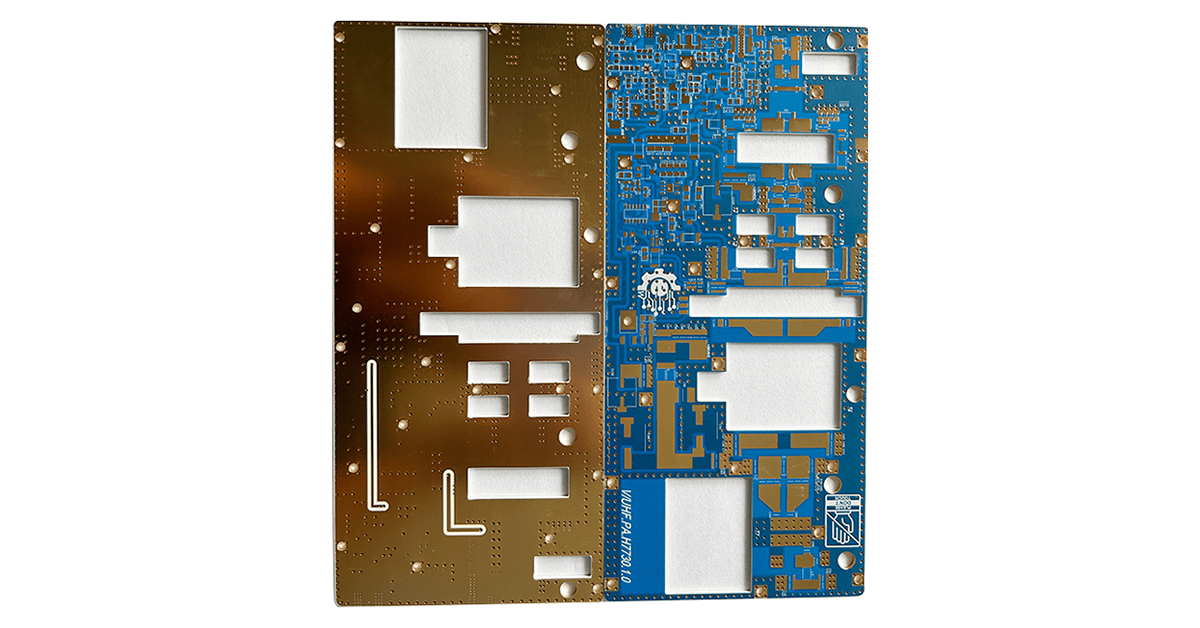
Why RO4350B Processes Like FR-4 (and Where It Refuses To)
RO4350B is a ceramic-filled, thermoset hydrocarbon laminate — not a PTFE material. That single sentence defines the entire manufacturing strategy. Because there is no PTFE in the resin system, there is no sodium-naphthalene etching, no plasma activation, and no special PTH chemistry. Standard electroless copper deposition works directly on the hole wall. Panels cut, drill, image and etch on the same equipment an FR-4 shop already runs.
The discipline that remains is precision, not exotic chemistry: impedance-critical line widths, lamination parameters that respect a thermoset cure cycle, and one non-negotiable factory rule covered below. For the failure modes that appear when these are missed, see our RO4350B production problems analysis.
The Seven-Step RO4350B Process Flow
| Step | Process | The one thing that matters |
|---|---|---|
| 1. Cutting & inner-layer prep | Standard cutting; inner-layer copper gets oxide/browning treatment | Bond strength starts here — skip it and multilayer lamination delaminates |
| 2. Drilling | Standard FR-4 parameters, carbide bits | Clean hole walls — smear control protects plating adhesion |
| 3. Hole metallization (PTH) | Standard electroless copper, then panel or pattern plating | No PTFE activation needed — the biggest cost step saved |
| 4. Pattern transfer | Dry film or liquid photoresist, expose & develop | Exposure energy control holds fine-line width tolerance |
| 5. Etching | Alkaline etch | Line-width accuracy = impedance accuracy |
| 6. Solder mask & surface finish | Thorough cleaning, cure-compatible mask, ENIG typical | Finish choice affects RF conductor loss (see below) |
| 7. Profiling & RF test | CNC routing or V-score; electrical test + VNA | S21/S11 on critical channels, not just opens/shorts |
Drilling and Hole-Wall Quality
RO4350B drills with standard tungsten-carbide tooling at FR-4-class parameters, but the ceramic filler is more abrasive than epoxy resin. Tool life management matters: sharpened or new bits, controlled hit counts, and quality entry and backup materials keep hole walls clean and burr-free. Excessive smear or rough walls compromise hole-wall adhesion and plating uniformity, which shows up later as barrel cracks during thermal shock or reflow.
A desmear step is recommended — though its necessity is lower than for FR-4 — because it guarantees a chemically clean wall before electroless copper. This is the same drilling-and-desmear logic detailed in our hybrid lamination technology analysis.
Lamination Pressure and Cure Cycle
RO4350B is a thermoset: the laminate cures fully during the original press, and bonding multilayers is about interface chemistry and pressure discipline. Use moderate lamination pressure — excessive pressure can redistribute the ceramic filler and create local Dk variation across the panel, which is invisible until impedance testing. Optimize ramp rate and cure cycle for the bonding material in use.
Two supporting controls: browning/oxide treatment on inner-layer copper before pressing, and a pre-bake when incoming material has seen humidity (roughly 125 °C for 2 hours) to drive off moisture that would otherwise blister during the press or during assembly reflow.
Impedance Control in Production
The entire commercial reason for choosing RO4350B is signal integrity, so impedance control is the manufacturing centerpiece. Four physical variables set the final impedance: dielectric thickness, etched line width, copper weight and solder-mask thickness over the trace. Each needs its own control loop:
- Design phase: simulate with the right Dk value — process Dk is 3.48 ± 0.05, while Rogers’ design Dk for simulation is 3.66. Using the wrong one shifts predicted impedance before the first panel is ever etched.
- Etch phase: line-width tolerance is the dominant controllable variable; verify with microsection, not visual check.
- Verification: TDR impedance coupons on the production panel, every panel, not per lot. XCE PCB controls impedance to ±10% with coupon verification as standard.
The parameters-versus-production relationship is covered in more depth in our RO4350B parameters and production guide.
Surface Finish Selection
ENIG is the default recommendation — flat pads for fine-pitch RF components, excellent solderability, no solder-mask-on-pad risk. The quality caveat: low-grade ENIG risks black pad corrosion, a reliability failure that is hard to detect before assembly. Immersion silver and immersion tin are viable alternatives with lower conductor-loss penalties; both need attention to storage life. HASL is generally avoided on RF builds because its uneven, rough surface adds conductor loss at high frequency. The finish-versus-loss trade-off is quantified for automotive radar in our radar applications article, and the ENIG nickel-layer physics in our immersion-gold analysis.
The One Factory Rule: Never Share the PTH Line With PTFE
RO4350B needs no dedicated line — but it needs a clean one. The specialized chemistries used to activate PTFE materials (sodium-naphthalene or plasma-era processes for laminates like RO5880) must never contact RO4350B panels. Cross-contamination of the electroless copper bath or the activation residues on panels lead to adhesion failures that surface as voids in plated through-holes. Shops running both material families segregate the PTH lines as standard practice.
RF Acceptance Testing: What Ships and What Does Not
Standard opens/shorts electrical test confirms connectivity; it says nothing about RF performance. Production acceptance on RO4350B builds adds vector network analyzer (VNA) measurement of insertion loss (S21) and return loss (S11) on critical channels, against limits agreed at design handoff. Combined with TDR impedance coupons and microsection analysis, this closes the loop between the datasheet the designer simulated with and the board the assembler receives.
How XCE PCB Builds RO4350B
XCE PCB runs RO4350B from 2 to 72 layers, impedance controlled to ±10% and verified with TDR coupons on every production panel, panels up to 600 × 1200 mm, and samples in as fast as 24 hours when laminate is in stock. PTFE and RO4000-family lines are segregated. For the failure modes this process prevents, read the production problems analysis; for the material itself versus its 4003C sibling, see the 4350B vs 4003C comparison.
Frequently Asked Questions
Does RO4350B require plasma treatment or sodium etching like PTFE laminates?
What impedance tolerance is realistic on RO4350B boards?
Can RO4350B and PTFE materials run on the same production line?
Why is pre-baking recommended before assembly?
Which surface finish is best for RF RO4350B boards?
Need RO4350B Boards Built to RF Tolerance?
Send us your Gerber files and requirements for a manufacturability review and a tailored quotation.
sales1@xcepcb.com
+86 180 3341 4657