
Seven steps, four environmental controls, and the special rules RF boards demand — how finished boards leave our factory protected.
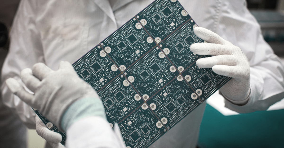
Packaging High-Frequency PCBs: The Short Answer
Bottom line up front: a finished high-frequency PCB is not finished until it survives shipping and storage. Packaging follows seven steps — cleaning, static protection, layer separation, labeling, sealing, transport preparation, and documentation — plus a set of considerations around moisture, temperature, and handling. RF boards add special requirements: no conductive materials, no volatile organic compounds (VOCs), and extra shock protection for high-value builds.
This article walks through the complete packaging procedure our production team applies before any high-frequency board leaves the factory.
The Seven Packaging Steps
Every order follows the same sequence:
| Step | What is done | Why it matters |
|---|---|---|
| 1. Surface cleaning | Remove dust, dirt, and residues from the PCB surface | Prevents damage during transport and storage |
| 2. Static protection | Wrap boards in anti-static bags or anti-static foam | Prevents electrostatic discharge (ESD) damage |
| 3. Layered packaging | Isolation foam or plastic dividers between boards | No direct board-to-board contact; fewer scratches |
| 4. Labeling | Contents, quantity, production date, specs, precautions on every box | Fast identification in transit and warehouse |
| 5. Sealed packaging | Bubble wrap and packing tape seal the box | Keeps moisture, dust, and contaminants out |
| 6. Transport prep | Sturdy cardboard or wooden crates matched to the mode of transport | Withstands impacts and pressure in transit |
| 7. Documentation | Production records, inspection reports, certificates attached | Quality tracking and verification downstream |
The order matters: cleaning before static protection, separation before sealing, and documentation last so it reflects the final, inspected contents.
Considerations: Environment and Handling
Four conditions determine whether packaging actually protects the boards:
- Moisture control: moisture-proof packaging materials are selected especially for high-humidity destinations — absorbed moisture ages materials and degrades performance.
- Temperature control: shipments through extreme temperature conditions get appropriate protection so boards are not affected by heat or cold.
- Transportation conditions: a reliable carrier and measures against severe vibration and impact minimize damage risk in transit.
- Storage environment: dry, cool, well-ventilated storage away from direct sunlight and humidity.
Labels and markings must be unambiguous throughout — handling and receiving staff depend on them at every hand-off.
Special Requirements for High-Frequency Boards
RF assemblies add a stricter packaging rule set:
- Material choice: avoid conductive packaging materials or those containing volatile organic compounds (VOCs) — anything that might affect signal transmission or contaminate the laminate surface.
- Shock protection: high-value or fragile boards get additional shock-absorbing materials — bubble wrap, foam padding, or custom protective frames.
- Modular packaging: for boards destined for larger systems, packaging each module separately simplifies assembly and replacement and reduces the risk of damage to the whole unit.
Inspection and Confirmation Before Shipping
Packaging ends with verification, not tape:
- Packaging inspection: a final check that all boards are correctly packaged and clearly labeled — no omissions, no errors.
- Quantity confirmation: the count inside the box is matched against the shipping order to avoid delivery disputes.
- Transportation confirmation: expected arrival time, routes, and safety measures confirmed with the carrier before hand-off.
- Receiving and feedback: on arrival, packaging is inspected for damage; any issues are documented and fed back to production and QC to improve the process.
Why Packaging Discipline Matters for RF Boards
A high-frequency board can pass every electrical test at the factory and still arrive degraded: micro-scratched RF traces, ESD-damaged pads, moisture uptake shifting dielectric behavior, or contaminated gold fingers. None of this shows on a packing slip — it shows at assembly or, worse, in the field. That is why packaging is treated as part of production, not an afterthought.
XCE PCB ships high-frequency boards from 2 to 72 layers with impedance held to ±10% and prototypes in as fast as 24 hours — packed to the standard above, wherever they ship.
Conclusion
Good packaging is a seven-step sequence plus four environmental considerations and a stricter rule set for RF: no conductive or VOC-containing materials, real shock protection, and modular packing for system boards. The final inspection loop — packaging check, quantity match, carrier confirmation, and receiving feedback — closes the quality chain from production floor to your assembly line. If you need high-frequency boards packed and shipped to spec, send us your requirements; we will confirm the packaging plan with your quote.
Frequently Asked Questions
Why do high-frequency PCBs need anti-static packaging?
What packaging materials should never touch an RF board?
How do you protect PCBs from moisture during shipping?
How are multiple PCBs packed in one shipment?
What happens if the packaging arrives damaged?
Need RF Boards Packed and Shipped to Spec?
Send us your Gerber files and requirements for a manufacturability review and a tailored quotation.
sales1@xcepcb.com
+86 180 3341 4657