
An HDI board is not made of one material, and this is where most discussions of HDI materials go wrong. It is made of a core, of prepreg, of a build-up dielectric film and of copper foil, and each of those four has its own datasheet, its own supplier and its own tolerances. The earlier version of this article listed six substrates — FR-4, RO4350B, RO4003C, PTFE, high-Tg FR-4, polyimide — as if choosing one of them were the material decision, and got the electrical parameters of four of them wrong. The properties that actually decide an HDI build are the ones that survive eight press cycles and three reflows, and the loss that matters most sits in the layer nobody specifies: the 60–80 µm build-up film.
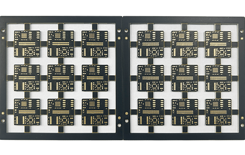
Four Materials, Four Datasheets
The build-up construction of HDI separates the board into a finished core, which can be any laminate at any thickness the design needs, and one or two thin dielectric layers laminated onto each side of it. That separation is a materials opportunity: the core can be a low-loss RF laminate while the build-up layers are cheap epoxy, or the core can be ordinary FR-4 while the build-up layers carry the fine routing. It is also a trap, because a datasheet quoted for a core laminate says nothing about the film twenty micrometres above it.
| Layer | What it is | Cured thickness | The parameter that matters | Who chooses it |
|---|---|---|---|---|
| Core | Cured laminate with copper on both faces | 0.1–1.0 mm | Dk and Df if RF signals run on it | Designer, from the electrical requirement |
| Prepreg | B-stage glass fabric with partially cured resin | 0.05–0.19 mm after press | Resin content, flow, and the thickness it leaves behind | Fabricator, from the stack-up |
| Build-up film | Resin-coated copper or resin film, laser-drillable | 60–80 µm | Df, laser absorption, CTE, dielectric strength | Fabricator, within the customers' loss budget |
| Copper foil | ED, rolled or reverse-treated, 9–35 µm | as supplied | Surface roughness Rz for conductor loss; elongation for fine lines | Designer, by specifying foil class |
The table already contains the answer to the question this article is named after. The material that decides whether an HDI board is an RF board is the core. The material that decides how much loss the digital layers have is the film. And the material that most often arrives without a specification is the prepreg, which is where thickness errors of 10 % get introduced.
What HDI Materials Have to Survive
The selection criteria for HDI are process criteria before they are electrical ones, because the board is pressed repeatedly and then soldered. Four requirements come from the process itself, and each maps to a parameter that has to be on the datasheet.
Temperature: a lead-free reflow peaks at 245 °C, so the material sees roughly 260 °C of short-term excursion, and a double-sided assembly sees it twice per side. That is a Tg question — a laminate with Tg 135 spends the top of the profile above its glass transition, where Z expansion triples — and a Td question for repeated cycles. Thermal expansion: the same Z movement strains every plated barrel, and on a thin HDI board the aspect ratio of the through holes in the core is high, so the strain budget is tighter than on a thick board. Moisture: absorbed water flashes to steam at reflow and delaminates the build-up film if the dry-out before press and before assembly is wrong, which makes moisture absorption a press parameter as much as a material one. And ionic cleanliness: on 50 µm lines the spacing between conductors is small enough for electrochemical migration, so resin chemistry and process residues become reliability variables rather than cosmetic ones.
Those four requirements are the reason high-Tg FR-4 exists and the reason the “high Tg” number on its own is not a specification. The measurement caveat — DSC, TMA and DMA give three different answers for the same board — is covered in glass transition temperature.
The Core: Where the RF Performance Is Decided
If the antenna feed or the transmission line runs on the core, the core laminate is the electrical decision, and its two numbers are Dk and Df. The table below gives the current datasheet values for the materials that appear in HDI radio designs, and it is worth comparing against the values printed in supplier articles, several of which are wrong by enough to change a design.
| Laminate | Dk (process) | Df at 10 GHz | Tg or Td | k, W/m·K | CTE Z, ppm/K |
|---|---|---|---|---|---|
| FR-4, standard | 4.2–4.6 at 1 MHz | 0.018–0.025 at 1 MHz | Tg 130–140 | 0.25–0.30 | 50–70 |
| FR-4, high Tg | 4.2–4.6 at 1 MHz | 0.018–0.025 at 1 MHz | Tg 170–180, Td 340+ | 0.30–0.40 | 45–60 |
| RO4350B | 3.48 ±0.05 (design 3.66) | 0.0037 | Tg >280, Td 390 | 0.69 | 32 |
| RO4003C | 3.38 ±0.05 (design 3.55) | 0.0027 | Tg >280, Td 425 | 0.71 | 46 |
| RO3003 | 3.00 ±0.04 | 0.0010 | Td 500 | 0.50 | 25 |
| RO3010 | 10.2 ±0.30 | 0.0022 | Td 500 | 0.95 | 16 |
| RT/duroid 5880 | 2.20 ±0.02 | 0.0009 | Td >500 | 0.20 | 237 |
| Taconic TLY-5 | 2.20 ±0.02 | 0.0009 | Tm ≈327, no Tg | 0.22 | 217 |
Three remarks on the table. First, the FR-4 numbers are quoted at 1 MHz and the RF numbers at 10 GHz; comparing them directly understates the FR-4 loss at microwave frequencies, where Df rises with frequency. Second, the design Dk of RO4350B and RO4003C is not the process Dk — 3.66 and 3.55 against 3.48 and 3.38 — and impedance synthesis has to use the design value while acceptance coupons measure the process value. Third, the Z-axis CTE column is what makes PTFE cores awkward in an HDI build: 217–237 ppm/K against 17 for copper means the plated through holes in the core, not the microvias, become the reliability item.
Where a PTFE core is chosen for loss, the details of its construction matter as much as the numbers; the 5880 family is set out in RT/duroid 5880 parameters and production guidelines.
The Build-Up Dielectric: The Loss Nobody Specifies
Build-up films are formulated to be laser-drillable, to fill, to adhere and to survive press, and their electrical performance is a secondary requirement. The consequence is a dissipation factor of 0.015–0.025 and a Dk of 3.3–3.6 — broadly the same dielectric constant as FR-4, and a loss four to eight times worse than a hydrocarbon RF laminate.
The practical use of that number is the attenuation formula for dielectric loss, αd ≈ 2.6 · fGHz · √Dk · Df in dB/inch. On a 75 µm build-up film at Dk 3.4 and Df 0.02 it gives about 0.96 dB/inch at 10 GHz. The same arithmetic on the core materials gives 0.18 dB/inch for RO4350B, 0.13 for RO4003C and 0.035 for 5880.
| Dielectric | Dk | Df | Dielectric loss at 10 GHz | Relative to 4350B |
|---|---|---|---|---|
| Build-up film | 3.4 | 0.020 | 0.96 dB/in | 5.2× |
| Build-up film, low loss grade | 3.3 | 0.010 | 0.47 dB/in | 2.6× |
| FR-4 | 4.4 | 0.020 | 1.08 dB/in | 5.9× |
| RO4350B | 3.48 | 0.0037 | 0.18 dB/in | 1× |
| RO4003C | 3.38 | 0.0027 | 0.13 dB/in | 0.7× |
| RT/duroid 5880 | 2.20 | 0.0009 | 0.035 dB/in | 0.19× |
Note what the table does and does not say. It says that a 50 Ω line on a build-up layer loses about a decibel per inch at 10 GHz, which is acceptable for a 30 mm digital escape and disastrous for a 100 mm antenna feed. It does not say that build-up layers are unusable for RF — low-loss grades at Df 0.010 halve the figure — but it does explain the standard architecture of an HDI radio module: radio on the core, digital in the build-up.
Frequency Dependence: A Df from 1 MHz Is Not a Df
Most FR-4 datasheets quote Dk and Df at 1 MHz, and most RF laminates quote them at 10 GHz, and the two are not interchangeable. Loss rises with frequency for every organic dielectric; what differs is the slope. Epoxy loses its figure by a factor of two or more between 1 MHz and 10 GHz, which is why an FR-4 quoted at 0.020 at 1 MHz behaves like 0.02 or worse at 10 GHz with a corresponding attenuation of about 1 dB/inch, while PTFE is nearly flat and keeps its 0.0009 across the band.
Two practical rules follow. Always ask for Dk and Df at the frequency the circuit runs at, and treat a number with no frequency as unusable for design. And when comparing two laminates, compare them at the same frequency: a hydrocarbon at 0.0037 at 10 GHz against an FR-4 at 0.020 at 1 MHz understates the gap, because the FR-4 figure at 10 GHz is worse than the one printed.
The same caveat applies to Dk, and it is the reason the design Dk of RO4350B (3.66) differs from its process Dk (3.48): the process value is measured with a fixture at a stated frequency, and the design value is the one that reproduces measured impedance across a band. Confusing the two is a common cause of a stack that measures 3 % off on first article — the arithmetic is in impedance control in high-frequency PCB manufacturing.
Prepreg: The Thickness Nobody Specifies
Prepreg is B-stage glass fabric with partially cured resin, and after pressing it becomes the dielectric between core layers. Its thickness after cure is not the same as before, because resin flows out of the weave under pressure, and the amount that flows depends on resin content and on the press cycle. That is why the same nominal prepreg can produce different dielectric thicknesses at two fabricators, and why dielectric thickness tolerance of ±10 % is the realistic figure rather than ±5 %.
| Style | Resin content | Thickness after press | Typical role |
|---|---|---|---|
| 106 | 70–76 % | 0.05 mm | Thin bond line, high resin to fill fine features |
| 1080 | 63–68 % | 0.065–0.08 mm | The workhorse for controlled-thickness bonds |
| 2116 | 52–58 % | 0.10–0.12 mm | Standard multilayer dielectric |
| 7628 | 42–48 % | 0.17–0.19 mm | Thick dielectric, low resin flow |
For HDI there are two extra requirements on prepreg that do not appear on a conventional board. Resin flow has to be enough to fill the copper features of the layer below without starving the bond line, which is why high-resin styles like 106 and 1080 are used next to fine-line layers; and the cured thickness has to be known because it sets the impedance of any stripline in the core. That is the mechanism by which impedance moves without anyone changing a drawing, and it is one of the reasons lamination is the step where tolerances accumulate — see lamination in high-frequency PCB for the press windows.
Copper Foil: Rz, Skin Depth and the Conductor Term
At 10 GHz the current in copper occupies the outer 0.65 µm, so a foil whose surface profile is 5 µm high forces the current to follow a path several times longer than the straight line. The parameter is Rz, and it is specified by foil class rather than by weight.
| Foil class | Rz, µm | Where it is used | Effect at 10 GHz |
|---|---|---|---|
| Standard ED | 5–8 | General digital, power | Conductor loss 20–40 % above smooth-foil values |
| Reverse-treated (RTF) | 3–5 | Fine line, inner layers | Middle of the range, good adhesion |
| HVLP / VLP | 1.5–2.5 | High-frequency outer layers | Lowest conductor loss; adhesion depends on treatment chemistry |
| Rolled annealed (RA) | 1–3 | Flexible and dynamic applications | Smooth and ductile; higher cost |
Two consequences for HDI. On a build-up layer, the foil is often supplied already coated with resin, and the foil class is fixed by the film product rather than chosen — which is another reason the build-up layer is not the place to design a low-loss line. And on fine lines, foil thickness and roughness interact with etch: a 9 µm foil etches far better than 35 µm at 50 µm lines, which is why thin foil is a capability requirement rather than a cost decision. The copper side of the argument, including current capacity by weight, is in PCB copper thickness.
Where the Earlier Version Had the Numbers Wrong
The previous version of this article listed six materials with parameters, and four of the six sets were wrong — two of them by enough to change a stack. This is the same error pattern that appears across supplier pages: one laminate's numbers copied onto another.
| Material | Value in the original | Datasheet value | Consequence if used |
|---|---|---|---|
| RO4350B Dk | 2.55 ±0.05 | 3.48 ±0.05, design 3.66 | A 50 Ω line would be drawn about 40 % too wide |
| RO4350B CTE | 30 ppm/K | 10 / 12 / 32 (X / Y / Z) | Hides the Z figure, which is the one that strains vias |
| RO4003C Df | 0.0035 | 0.0027 | Overstates loss by 30 %, in the safe direction |
| RO4003C CTE | 18 ppm/K | 11 / 14 / 46 | 18 is close to copper and would remove the reliability concern that actually applies |
| PTFE Df | < 0.0002 | 0.0009 for RT/duroid 5880 | Promises a loss four times better than achievable |
| PTFE Dk | about 2.1 | 2.20 ±0.02 | Minor, but it propagates through every width calculation |
| FR-4 Dk / Df | 4.0–5.0 / 0.02–0.03 | 4.2–4.6 / 0.018–0.025 at 1 MHz | Ranges too wide to design with; no frequency stated |
| Polyimide | listed as an HDI substrate | A film for flex and coverlay, not a rigid core | Category error: rigid HDI cores are glass-reinforced |
Two structural errors sit behind the numeric ones. The original described “ROGERS” as a substrate material, which confuses a manufacturer with a chemistry — RO4350B and RO4003C are hydrocarbon/ceramic thermosets, while RT/duroid 5880 is PTFE with micro-glass, and the two families have different press windows, different drilling behaviour and different desmear chemistry. And it treated the choice of one laminate as the whole material decision, when the build-up film above it has ten times the loss.
The Other Properties That Matter, and Where They Are Specified
Four parameters rarely quoted in marketing copy decide whether an HDI stack survives. Peel strength: the copper-to-dielectric bond has to hold through press and reflow, and it is measured in N/mm; RO4350B is about 1.05 N/mm and 5880 about 5.5 N/mm, a factor of five that changes how the surface is treated before bonding. Moisture absorption: 0.02 % on PTFE against 0.06 % on RO4003C and 0.1–0.2 % on FR-4, which sets the bake before press. Dielectric strength: relevant because the build-up film is thin, so 75 µm of film carrying 100 V is a field of 1.3 kV/mm, still far below breakdown but no longer negligible. And CAF resistance: on 50 µm lines at 50 µm spacing, electrochemical migration between conductors becomes a qualification test rather than a footnote.
None of these appears in a headline specification, and each of them can fail a build on its own. The general framework for what these numbers mean for insulation, including the difference between dielectric strength as a material property and as a board property, is in properties and role of insulation.
Selection by Function, Not by Family
The material decision in an HDI design is really a decision about which layers carry which signals. Once that is stated, the materials follow.
| Function of the layer | Requirement | Material | What to specify |
|---|---|---|---|
| Digital escape and power on build-up | Fine lines, laser drillability | Standard build-up film | Thickness 60–80 µm, Df class, CTE |
| Antenna feed and filters | Df at the operating frequency | PTFE or hydrocarbon core | Dk tolerance, Df, TCDk |
| Mixed RF and digital in one core | Loss where it matters, cost elsewhere | Two cores in one stack | Press compatibility of both systems |
| High-current or thermal pad | Heat and current | Thick copper, filled vias, high-k laminate | k, copper weight, via fill |
| Automotive or industrial | Thermal cycling | High Tg FR-4 or hydrocarbon | Tg by stated method, Td, Z CTE, reflow count |
The mixed row deserves emphasis because it is where most programmes save money. Two cores in one stack — a small piece of PTFE or hydrocarbon where the radio sits, FR-4 everywhere else — is a lamination challenge rather than a materials one, and the constraint that governs it is that the press windows differ: FR-4 at 170–190 °C, RO4000 at 190–200 °C, PTFE with FEP at 260–300 °C. They cannot be co-pressed in one cycle, which is why hybrid stacks are pressed in stages or bonded with a transition prepreg.
The Material Callout for an HDI Enquiry
Six items make the material part of an HDI enquiry unambiguous, and each corresponds to a failure mode. The core laminate by trade name and construction, with Dk and Df and the frequency they are quoted at. The core thickness after press, not the prepreg thickness. The build-up film by product and thickness, with the Df class. The copper foil class per layer, since Rz is what sets conductor loss. The Tg measured by a stated method, with Td. And the press and reflow cycle count the board has to survive, because that, not the ambient temperature, is what the CTE numbers are being used for.
XCE PCB holds 2 to 72 layers, panels to 600×1200 mm, impedance to ±10 % and samples in as fast as 24 hours, and builds HDI on FR-4, hydrocarbon and PTFE cores with the corresponding bonding systems. The build-up structure itself — how many layers, how the vias are stacked — is the subject of the detailed introduction to HDI PCB, and the process windows that follow from these materials are in HDI PCB manufacturing process.
Conclusion
HDI materials are four materials, and the datasheet that decides the electrical result is the core: RO4350B at Dk 3.48 and Df 0.0037, RO4003C at 3.38 and 0.0027, RT/duroid 5880 at 2.20 and 0.0009. The layer directly above them is a 60–80 µm build-up film with Df 0.015–0.025, which at 10 GHz costs about 0.96 dB/inch against 0.18 for 4350B and 0.035 for 5880 — a factor of five to twenty-seven that no via scheme recovers. The prepreg decides the thickness of the core dielectric and therefore the impedance, with ±10 % variation that comes from resin flow rather than from the press. The foil decides the conductor term through Rz, 5–8 µm on standard ED against 1.5–2.5 on HVLP.
The one sentence worth carrying into a design review: put the radio on the core and the digital in the build-up, and specify the build-up film's Df the same way you specify the core's. Everything else in this article is the arithmetic that supports it.
Frequently Asked Questions
What is the Dk of RO4350B?
Why do build-up layers have worse loss than the core?
Is polyimide an HDI substrate?
How much does prepreg thickness vary, and why?
What copper foil should be specified for a 10 GHz layer?
Can a PTFE core and FR-4 build-up be pressed together?
Need a Build-Up Stack With the Core Material You Actually Want?
Send us your Gerber files and requirements for a manufacturability review and a tailored quotation.
sales1@xcepcb.com
+86 180 3341 4657