
Thermal management in PCB manufacturing is usually described with adjectives — excellent, superior, high-performance — and the earlier version of this article was a list of them: thermal conductivity, thermal resistance, heat capacity, CTE, and a second “thermal resistance” that meant something else entirely. None of it could be calculated with. The performance of a thermal design is five numbers — conductivity k, thermal resistance per unit area R″ = t/k, structure resistance θ, expansion coefficient CTE and the two temperature limits Tg and Td — and its role is the management of a chain of resistances between a junction and the air. This article gives the arithmetic for each, the values for the laminates actually used, and the six claims in the original that do not survive measurement.
Five Numbers Instead of Five Adjectives
The performance of thermal management is not a quality of a board, it is a set of measurable quantities, and each answers a different question. Conductivity says how well a material passes heat. Resistance per unit area says how much temperature that material costs you at a given thickness. Structure resistance says how much temperature the path costs you between the die and the air. CTE says whether the assembly will survive the excursion to reflow, and Tg and Td say what the laminate can be put through before it stops being the same material.
| Quantity | Symbol and unit | What it answers | Typical range on a PCB |
|---|---|---|---|
| Thermal conductivity | k, W/m·K | Material property: heat per metre of thickness per kelvin | 0.20 (PTFE) to 1.44 (ceramic-filled), copper 385 |
| Thermal resistance per unit area | R″, K·cm²/W | What the dielectric thickness costs at a given flux | 1.8 to 12.7 for 0.254 mm of laminate |
| Structure thermal resistance | θ, K/W | What the whole path costs for a given power | 5 to 300, dominated by the weakest link |
| Coefficient of thermal expansion | CTE, ppm/K | Reliability, not cooling: how far things move when hot | Cu 17, Z-axis FR-4 50–70, PTFE 217–237 |
| Temperature limits | Tg, Td, °C | What processing the laminate survives | Tg 130–180 (FR-4), Td 300–425 |
Everything below is either a value of one of these five, or an arithmetic relation between them. A sentence about thermal management that contains none of them is a sentence that cannot be checked, and those sentences are what the original article consisted of.
What the Original Version Got Wrong
The earlier draft had the right topics and the wrong content: no number anywhere, one term used for two different quantities, and three claims that reverse the engineering. They are listed here because the same six phrases appear on most supplier pages.
| Statement in the original | What is actually true |
|---|---|
| Thermal resistance appears twice in the list of properties | Two different quantities were merged. Thermal resistance (θ, K/W, or R″, K·cm²/W) is a path property and is what you calculate with. Heat resistance is a material limit — Td, Tg, UL RTI — and is a temperature, not a resistance |
| Matching CTE reduces thermal stress | Matching is not available. Copper is 17 ppm/K; FR-4 is 50–70 in Z; PTFE laminates are 217–237 in Z, which is 13–14 times copper. The work is in managing the mismatch — symmetric stacks, ductile plating, aspect ratio — not in eliminating it |
| Thermal management reduces signal loss | It does not, and the causality runs the other way: temperature changes Dk and Df, which changes loss and phase. Keeping a board cool protects electrical stability; it does not remove attenuation |
| Heat capacity absorbs heat and evens out fluctuations | Heat capacity matters only in transients lasting seconds. A 1.6 mm FR-4 board is about 1.9 J per cm³ per K; a 10 cm² section is roughly 3 J/K, which is the energy of 1 W for three seconds. It is never a steady-state argument |
| High-conductivity materials such as copper and aluminium solve it | A laminate is not a metal. Where an aluminium base is used, the bottleneck is the 75–100 µm dielectric layer at 1–3 W/m·K, not the 205 W/m·K core. That layer, being thin, is why metal-core boards work at all: 0.5 K·cm²/W against 8.5 for 0.254 mm of FR-4 |
| Thermal management prevents fire and explosion, and improves space utilisation | Board-level heat spreading is not a safety function; fire safety comes from component derating and enclosure design. “Space utilisation” has no measurable content unless it is stated as copper area, via count or spreader footprint |
Three of the six are vocabulary errors and three are reversed causalities. Together they explain why the original could be read in full without learning anything actionable, which is the actual failure mode of most pages on this subject.
The Heat Path: Five Resistances in Series
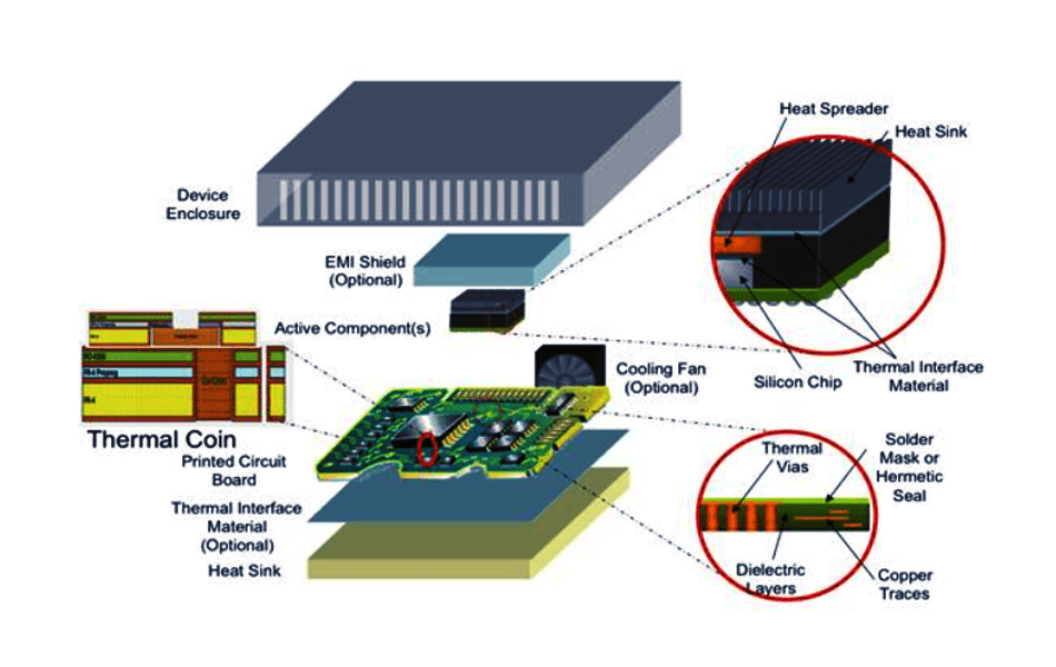
Heat leaves a junction by one route at a time, and each section of that route adds resistance. In series they add; θJA = θJC + θinterface + θboard + θspreader + θambient. Two consequences follow immediately. The largest term sets the result, so improving the second largest is invisible; and the board terms are usually not the largest, which is why adding copper to a badly interfaced design changes nothing.
A numeric example makes the ordering clear. Take a 0.254 mm laminate with 3 × 3 mm of contact area and a 25 µm plating in the vias. Through the dielectric alone the resistance is t/(kA): 0.000254 m divided by (0.71 W/m·K × 9 mm²) gives about 40 K/W. Nine 0.25 mm copper-filled vias under the same pad give 85/9, about 9 K/W. A single 1 oz plane spreading two squares sideways adds about 150 K/W. Natural convection off 1000 mm² at 10 W/m²·K adds about 100 K/W.
The ordering in that example — spreader, then convection, then dielectric, then vias — is typical, and it is the opposite of the ordering implied by most material tables. The laminate conductivity is the number buyers ask about and the number that decides the result least often.
k: The Smallest Number in the Chain
Thermal conductivity of the laminates used in high-frequency work spans a factor of seven, from 0.20 to 1.44 W/m·K. For comparison, copper is 385 and aluminium 205. That factor of seven is real and worth having, but it is applied to a layer that is only 0.1–0.8 mm thick, which is what the next section is about.
| Material | k, W/m·K | Df at 10 GHz | Where the number comes from |
|---|---|---|---|
| Copper (deposited) | 385 | n/a | Reference value, not a laminate property |
| Aluminium | 205 | n/a | Metal-core substrates |
| FR-4, standard | 0.25–0.30 | 0.018–0.025 | Epoxy/glass, the baseline |
| FR-4, high Tg | 0.30–0.40 | 0.018–0.025 | More aromatic resin, slightly better k |
| RT/duroid 5880 | 0.20 | 0.0009 | PTFE with micro-glass; the electrical benchmark and the thermal floor |
| Taconic TLY-5 | 0.22 | 0.0009 | Same family, same limitation |
| RO3003 | 0.50 | 0.0010 | Ceramic-filled PTFE |
| RO4003C | 0.71 | 0.0027 | Hydrocarbon/ceramic thermoset |
| RO4350B | 0.69 | 0.0037 | Same family, FR-4 process |
| RO3010 | 0.95 | 0.0022 | High Dk, high ceramic load, hence higher k |
| RT/duroid 6035HTC | 1.44 | 0.0013 | The high-thermal option: low loss and high k together |
The table has one trap in it. A high Dk laminate is high in ceramic filler, and ceramic filler raises k — so RO3010 at Dk 10.2 is also the most conductive of the RO3000 family at 0.95. Choosing a high-Dk material for electrical reasons therefore improves the thermal path as a side effect, while choosing PTFE for electrical reasons makes it worse. That trade is the subject of the next two sections.
R″ = t/k: The Comparison That Decides a Laminate
Conductivity alone cannot be compared across a range, because a thin layer of a poor conductor can beat a thick layer of a good one. The comparable quantity is resistance per unit area, R″ = t/k, in K·cm²/W. Multiplied by a heat flux in W/cm² it gives a temperature rise directly, which is the number a design review can argue about.
| Laminate (0.254 mm) | k | R″, K·cm²/W | Rise at 10 W/cm² | Rise at 2 W/cm² |
|---|---|---|---|---|
| RT/duroid 6035HTC | 1.44 | 1.76 | 17.6 K | 3.5 K |
| RO3010 | 0.95 | 2.67 | 26.7 K | 5.3 K |
| RO4003C | 0.71 | 3.58 | 35.8 K | 7.2 K |
| RO4350B | 0.69 | 3.68 | 36.8 K | 7.4 K |
| FR-4, k 0.30 | 0.30 | 8.47 | 84.7 K | 16.9 K |
| RT/duroid 5880 | 0.20 | 12.7 | 127 K | 25.4 K |
| Aluminium base, 100 µm dielectric | 2.0 | 0.50 | 5.0 K | 1.0 K |
Two readings matter. First, the aluminium-base row, which is the best in the table by a factor of three over 6035HTC and by a factor of 25 over 5880, achieves that with a dielectric that is thinner rather than more conductive — 100 µm of 2 W/m·K beats 254 µm of 1.44. Second, thickness is the lever with the same authority as material: on RO4350B, dropping from 0.508 mm to 0.127 mm halves R″ and doubles the temperature. This is why a thermal problem on a high-frequency board is often solved by a thinner core at the same Dk rather than by a different family.
The same arithmetic runs the other way for insulation. Reducing dielectric thickness for thermal reasons also reduces dielectric strength and increases capacitance, so the trade is bounded — and it is the same trade discussed in the properties and role of insulation, where thickness appears as a voltage limit rather than a thermal one.
Thermal Vias: Where the Resistance Really Is
A via is a copper cylinder, so its resistance is L/(kA) with A being the copper cross-section, not the drill diameter. A 25 µm plated wall on a 0.2 mm hole gives 0.0157 mm² of copper; a filled via gives 0.031 mm². That factor of two is the whole difference between a plated and a filled thermal via, and it is usually presented as a mystery.
| Via, 1.6 mm board | Copper area | θ for one via | 9-via array | Comment |
|---|---|---|---|---|
| 0.10 mm, 25 µm wall | 0.0079 mm² | 529 K/W | 59 K/W | A microvia used as a thermal via is a poor conductor |
| 0.20 mm, 25 µm wall | 0.0157 mm² | 264 K/W | 29 K/W | Standard plated through via |
| 0.25 mm, 25 µm wall | 0.0196 mm² | 212 K/W | 24 K/W | Aspect ratio 6.4:1, near the practical limit |
| 0.20 mm, filled | 0.0314 mm² | 132 K/W | 15 K/W | Filled and capped, also planar for assembly |
| 0.25 mm, filled | 0.0491 mm² | 85 K/W | 9 K/W | The usual choice under a power pad |
| Same 1.44 mm² footprint, through FR-4 | 2.07 mm² of 0.3 W/m·K | 2 580 K/W | n/a | Why an unfilled via field beats no vias by two orders of magnitude |
The last row is the one worth remembering. A field of nine filled vias is roughly 275 times better than the laminate it passes through, which is why the presence of vias matters enormously and the choice between 0.2 and 0.25 mm does not. It also explains a common failure mode: a design with a large thermal pad, no vias and a thicker copper layer, improved in the wrong place.
The rule follows from the geometry: vias are a path, and a path is only useful if it lands on copper at both ends. A filled via ending on an inner signal layer is a dead end. Termination on a plane, or on a pad on the far side, is what completes the circuit — the same argument as in PCB through hole, where the via is discussed as a signal structure.
Copper as a Spreader: Per-Square Arithmetic
Copper spreads heat well but not infinitely well, and the quantity that makes this calculable is resistance per square in the plane. For a layer of thickness t, one square has R = 1/(k·t): 74 K/W for 1 oz, 37 K/W for 2 oz, 148 K/W for 0.5 oz. Squares in series add, and squares are counted in lengths of the path divided by its width.
A pad 5 mm wide feeding a spreader 20 mm away therefore crosses four squares: about 300 K/W on 1 oz copper. That number explains the empirical rule of thumb that heat stops spreading beyond 10–20 mm unless the plane is thick: the thermal resistance grows linearly with distance while the area available for convection grows only with the perimeter.
Three practical consequences. Copper thickness helps thermal spreading exactly as it helps current capacity, and for the same reason — cross-section — which is why heavy copper is used under power stages. Solder mask over copper costs little thermally (10–20 µm of polymer at 0.2 W/m·K is 0.1 K·cm²/W) but nothing at all electrically, so an exposed pad is about solderability rather than cooling. And the surface finish matters for neither, although it is often specified as if it did — the relevant comparisons are in surface treatment processes.
CTE: Matching Is Impossible, Managing Is Not
Expansion is where thermal management stops being about cooling and becomes about survival. The excursions that matter are not the operating ones but the assembly ones: a lead-free reflow peaks at 245 °C, so a board sees about 215 K above room temperature in a few minutes, and everything in the stack expands by its own CTE.
| Material | CTE X / Y / Z, ppm/K | Z expansion, 1.6 mm over 215 K | Consequence |
|---|---|---|---|
| Copper | 17 / 17 / 17 | about 6 µm | The reference everything else is measured against |
| RO4350B | 10 / 12 / 32 | about 11 µm | Closest to copper of the RF laminates |
| FR-4 (below Tg) | 14–17 / 14–17 / 50–70 | 17–24 µm, then a step above Tg | The step, not the slope, is the problem |
| RO4003C | 11 / 14 / 46 | about 16 µm | 2.7 times copper in Z |
| Taconic TLY-5 | 26 / 15 / 217 | about 75 µm | PTH strain becomes the design driver |
| RT/duroid 5880 | 31 / 48 / 237 | about 82 µm | 14 times copper; plating ductility is mandatory |
Since the barrel of a plated hole is copper and the laminate around it moves 4–14 times as far, the plating is strained in tension at every reflow. The controls are known and they are not material substitutions: plating elongation of at least 20 %, aspect ratio at or below 6:1 on PTFE, and a stack that is symmetric about the centre so the board does not bow. These are process rules, which is why they belong with lamination as much as with material selection.
Tg and Td: Two Limits That Are Not Operating Temperatures
The two temperature numbers on a datasheet are frequently read as a maximum operating temperature, which they are not. Tg is where the resin changes from glassy to rubbery: the CTE steps up, the modulus falls, and the Z expansion per kelvin roughly triples. Td is the decomposition temperature at 5 % weight loss, which is a chemical limit well above any soldering process.
What matters for a thermal design is the relationship between Tg and the process, not the ambient. A laminate with Tg 135 spends the top of a lead-free reflow above its glass transition and pays for it in Z expansion exactly where the vias are; a laminate with Tg 170–180 does not. Td enters only as margin against repeated excursions, and the practical check is cumulative reflow count rather than a single peak. The measurement caveat — DSC, TMA and DMA give different values for the same board — is covered in glass transition temperature.
For PTFE there is no meaningful Tg at all: the transition is around −120 °C, far below any service condition, and the laminate is above it at every temperature it will ever see. Its dimensional behaviour is governed by the PTFE CTE directly, which is why the previous section matters more on PTFE than on epoxy.
Temperature Drift of the Electrical Numbers
The role of thermal management in an RF board is not only to keep parts cool, it is to keep Dk where the design assumed it. Dk drifts with temperature at a rate given by TCDk, and the drift is signed — some laminates lose Dk as they heat, others gain it, and the sign decides which way a filter or a phased array walks.
| Laminate | TCDk, ppm/K | Dk change over 125 K | Phase drift, 100 mm at 10 GHz |
|---|---|---|---|
| RT/duroid 5880 | −125 | −1.6 % | about 14° |
| RO4003C | +40 | +0.5 % | about 5.5° |
| RO4350B | +50 | +0.6 % | about 7° |
| FR-4 | not specified, typically +100 to +300 | +1 to +4 % | not a controlled quantity |
The fourth column is the one that reaches a system specification: a phase shifter calibrated at 25 °C that drifts 14° at 100 °C is a different product. Note also that the drift is proportional to electrical length, so it is the length of the feed network rather than the size of the board that sets it. A thermally well-managed board and an electrically stable one are not the same thing, and the second requires knowing TCDk, not k.
Why High-Frequency Boards Are the Hard Case
The two properties that make a laminate good at 10 GHz — low Df and low Dk — both come from the same formulation choice: PTFE with micro-glass and almost no ceramic filler. That is also the formulation with the lowest conductivity in the table, 0.20 W/m·K, and the highest Z expansion, 237 ppm/K. The best electrical material is the worst thermal material, and no datasheet hides this: the two columns are adjacent.
Three strategies exist, and they are chosen by application rather than by preference. Put the loss-critical RF on PTFE and the dissipating digital on FR-4 in a hybrid stack, which is the usual answer and is a lamination problem as much as a material one. Accept a higher Df with better k, which is what 6035HTC at 1.44 W/m·K and Df 0.0013 is for. Or keep the PTFE and solve the thermal problem mechanically, with a metal back, thermal vias and a spreader — expensive but electrically neutral.
What does not work is the assumption that a low-loss laminate is also a cool one. On 5880 the dielectric alone costs 127 K at 10 W/cm², and since the loss per unit length on that material is about 0.035 dB/in at 10 GHz, the heat generated is small — which is why the thermal problem on PTFE boards comes from the components and the terminations, not from the transmission lines. Getting that distinction right is most of the design work.
Where Thermal Management Does Not Do What It Is Credited With
Four claims survive in marketing copy and do not survive a calculation.
| Claim | What actually happens |
|---|---|
| A thermally conductive laminate removes the need for a heat sink | It changes one term in a series chain. Going from FR-4 to 6035HTC reduces the dielectric term from 84.7 to 17.6 K·cm²/W; if convection is 100 K/W it remains the largest term and the improvement is a few kelvin at system level |
| More copper layers improve cooling | Only if they are planes connected by vias. Adding signal layers adds laminate — a second series resistance — and on PTFE adds it at 0.20 W/m·K |
| Thermal management lowers insertion loss | Temperature changes Dk and Df by the amounts in the previous section; keeping the board cool keeps the design at its nominal loss. Attenuation itself is set by Df and copper roughness |
| Surface finish choice affects heat transfer | Not measurably. A finish is 0.05–6 µm of metal or 0.2–0.5 µm of organics; its thermal resistance is negligible against 0.5 K·cm²/W for the thinnest dielectric in the stack |
The common structure of these four is the same as in the width and thickness arguments elsewhere on this site: a local material choice is being asked to fix a system-level problem whose largest term lies somewhere else. The diagnostic question is always “which term is largest, and by how much” — and with the tables above, that question has a numeric answer before any sample is ordered.
Selection by Heat Flux: A Matrix
Heat flux, not total power, is what separates the cases, because a small part with high flux and a large part with the same watts behave differently. The bands below are stated with the dielectric-temperature cost at 0.254 mm, so the material decision follows from the application rather than from a preference.
| Heat flux | Typical source | What decides it | Laminate and structure |
|---|---|---|---|
| < 0.5 W/cm² | Logic, low-power RF, small regulators | Nothing thermal; choose on Dk/Df | Any laminate, planes for return current |
| 0.5–2 W/cm² | Power amplifiers, LED strings, motor drivers | Copper area and via field | FR-4 with 2 oz planes, 0.3 mm thermal vias at 0.6 mm pitch |
| 2–5 W/cm² | GaN drivers, dense LED arrays | R″ of the dielectric becomes visible (7–17 K) | Thin core, filled vias, spreader; consider 6035HTC where RF is also present |
| 5–15 W/cm² | Bare-die, laser diodes, high-power RF | Dielectric R″ dominates (18–127 K) | High-k laminate or metal core; copper-filled via array under the die; forced air |
| > 15 W/cm² | IGBT modules, high-brightness laser | Not a laminate problem | Metal core or ceramic substrate, liquid or heat pipe, thermal interface material specified separately |
XCE PCB builds RF and mixed stacks across those bands: 2 to 72 layers, PTFE and hydrocarbon laminates with the corresponding bonding systems, copper-filled and resin-plugged vias, and impedance held to ±10 %. Where a hybrid is required, the press cycles are separate rather than combined, because the FR-4, RO4000 and PTFE/FEP systems do not share a window.
What to Specify and What to Test
Thermal requirements become controllable when they are written as five items, in the same way a width or an impedance becomes controllable. First, the laminate and its k at the operating temperature, with the thickness — because k alone does not fix R″. Second, the heat flux at the pad in W/cm², not the component power in watts. Third, the via structure under the pad: diameter, plated or filled, pitch and where the field terminates. Fourth, the copper serving as spreader: weight, area and continuity to the plane. Fifth, the CTE-driven rules for the process: plating elongation, aspect ratio, reflow count.
Testing follows the same list. A cross-section gives plating thickness and via fill; a thermal coupon measured on a hot plate gives R″ for the stack as built, which is the only number that includes the interface; and a reflow simulation to the actual peak gives the Z expansion and the strain in the barrel. None of these is a laminate datasheet test, and all three are cheaper than a field return.
The stack itself, including the via field and the plane assignment, is decided earlier — see high-frequency PCB stack-up design — and the copper weight that carries the current and spreads the heat is set with it, as covered in PCB copper thickness.
Conclusion
Thermal management in a PCB is a chain of five resistances and five material numbers, and its performance is calculable before a board exists. Conductivity ranges from 0.20 W/m·K on PTFE to 1.44 on 6035HTC; at 0.254 mm that is 12.7 against 1.76 K·cm²/W, or 127 K against 17.6 K at 10 W/cm². Structure resistance, not material, usually dominates: nine filled 0.25 mm vias are 9 K/W against 2 580 K/W for the laminate they pass through, and one square of 1 oz copper is 74 K/W in the plane. CTE is a reliability quantity, not a cooling one, and it cannot be matched to copper — PTFE is 14 times copper in Z, so the control is ductile plating and aspect ratio. Tg and Td are process limits, not operating temperatures.
The role of thermal management, stated in a way that can be checked, is this: keep the junction below its limit, keep the laminate inside the range where its Dk is the Dk the design used, and keep the plated barrels inside their strain budget across the reflow profile. Three objectives, five numbers, and no adjectives.
Frequently Asked Questions
How do I compare two laminates thermally?
Does a thermally conductive laminate remove the need for a heat sink?
Why do filled thermal vias work better than plated ones?
Can CTE be matched between laminate and copper?
Is a higher Tg always better for thermal performance?
How much does temperature move the electrical design?
Need the Thermal Path Designed, Not Assumed?
Send us your Gerber files and requirements for a manufacturability review and a tailored quotation.
sales1@xcepcb.com
+86 180 3341 4657