
Rogers 4360 is the shorthand for RO4360G2, a 6.15 dielectric constant laminate in the RO4000 family: glass-reinforced, hydrocarbon ceramic-filled, thermoset, and processed like FR-4. Almost every characteristic that matters downstream is a consequence of that one number. A 6.15 Dk shrinks a 50 Ω line by 35 % and shrinks the physical length of a wavelength by 22 %, which is the reason to buy it. It also doubles the sensitivity of that line to a 25 µm etch error, and it comes with the largest temperature coefficient of Dk in the family. This article works through the data sheet row by row, then puts numbers on both sides of the trade.
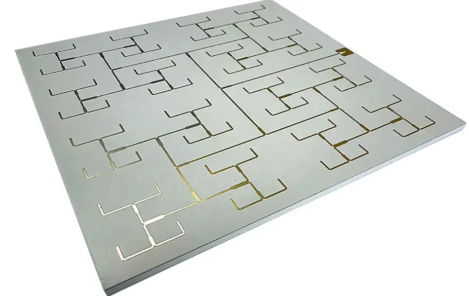
What “Rogers 4360” Actually Names
The part that is quoted as “Rogers 4360” is RO4360G2 in the current catalogue. The G2 suffix is not decoration: it is the second-generation formulation of a 6.15 Dk material, and it is the only version that should appear on a purchase order or a stack-up drawing. The older designation is still common in Chinese-language material lists, which is why boards are sometimes quoted against a part number that no longer has a data sheet behind it.
The construction matters more than the name. RO4360G2 is a glass-reinforced, hydrocarbon ceramic-filled thermoset — the same resin platform as RO4350B and RO4003C, with the ceramic loading pushed up until the dielectric constant reaches 6.15. It is not PTFE, it does not need sodium-naphthalene hole conditioning, and it does not need a 260 °C to 300 °C fusion cycle. It is laminated with RO4400 series prepreg at RO4000 conditions and drilled like an epoxy board. That is the whole point of the product: high Dk without PTFE processing.
One number on the data sheet is easy to miss and expensive to miss: design Dk 6.4 against process Dk 6.15. Rogers publishes both because the clamped-stripline test can read low when air is trapped at the fixture, and because real boards are not the fixture. The 4 % gap is larger than the ±0.15 tolerance on the process value, so a design modelled on 6.15 will come back reading low in impedance on a real coupon.
The Data Sheet, Row by Row
The table below is the RO4360G2 standard properties table, with the engineering consequence of each row rather than the marketing adjective. Where a number only means something in context, the context is in the fourth column.
| Property | Value | Condition | What it decides |
|---|---|---|---|
| Dk, process | 6.15 ±0.15 | 10 GHz, 23 °C, clamped stripline | Line width, wavelength, patch dimensions. The tolerance is ±2.4 % |
| Dk, design | 6.4 | Lot average, common thicknesses | What the model should use; 4 % above the process value |
| Df | 0.0038 | 10 GHz, 23 °C | Dielectric loss per wavelength. Low against FR-4, not low against 4003C |
| TCDk | -131 ppm/°C | -50 to +150 °C, 10 GHz | Centre-frequency drift of every resonator built on it |
| Thermal conductivity | 0.75 W/m·K | 50 °C, ASTM D5470 | Vertical thermal resistance: 3.39 K·cm²/W at 0.254 mm |
| CTE | 13 / 14 / 28 ppm/°C | -50 to 288 °C, X / Y / Z | PTH barrel strain; Z is 1.65× copper, not equal to it |
| Tg | 280 °C min | TMA | No softening in any reflow profile; quoted as “same as RO4000” |
| Td | 407 °C | TGA | Decomposition, not glass transition; sets the upper process limit |
| T288 | >30 min | 30 min / 125 °C prebake | Time to delamination at 288 °C; the number that matters for lead-free |
| Peel strength | 5.2 pli (0.91 N/mm) | 1 oz ED, condition B | Weakest of the RO4000 grades; fine-line etching needs the margin |
| Water absorption | 0.08 % | 50 °C / 48 h | About 4× a PTFE laminate; matters for humidity drift, not for reflow |
| Density | 2.16 g/cm³ | Room temperature | Weight per panel, and a proxy for ceramic loading |
| Dielectric strength | 784 V/mil (30.9 kV/mm) | Z direction | 7.8 kV across a 0.252 mm core, before derating |
| UL 94 | V-0 | File QMTS2.E102763 | The compliance item RO4003C cannot offer |
Two rows deserve a warning because they are the two that get misread. First, 0.0038 is not a low-loss number in absolute terms: it is roughly the same as RO4350B and 40 % higher than RO4003C. It is a low-loss number compared with FR-4 at 0.020, which is the comparison the data sheet is written against. Second, TCDk of -131 ppm/°C is a negative number of unusual size for this family — RO4350B is +50 and RO4003C is +40. A negative coefficient means the Dk falls as the board heats, so every resonator on the board drifts upward in frequency as it warms.
What Dk 6.15 Does to Geometry
For a 50 Ω microstrip the width is not a free choice: it is the dielectric height multiplied by a ratio that depends only on Dk. At 6.15 that ratio is about 1.47, against 2.27 for RO4350B and 3.08 for RT/duroid 5880. The table converts the standard core thicknesses into widths, and gives the guided wavelength at 10 GHz.
| Core (mm) | Tolerance | 50 Ω width | Wavelength at 10 GHz | Quarter wave |
|---|---|---|---|---|
| 0.203 | ±0.018 mm (±8.9 %) | 0.299 mm | 14.2 mm | 3.6 mm |
| 0.406 | ±0.038 mm (±9.4 %) | 0.598 mm | 14.2 mm | 3.6 mm |
| 0.508 | ±0.038 mm (±7.5 %) | 0.748 mm | 14.2 mm | 3.6 mm |
| 0.610 | ±0.038 mm (±6.2 %) | 0.898 mm | 14.2 mm | 3.6 mm |
| 0.813 | ±0.051 mm (±6.3 %) | 1.197 mm | 14.2 mm | 3.6 mm |
| 1.524 | ±0.102 mm (±6.7 %) | 2.244 mm | 14.2 mm | 3.6 mm |
The wavelength column is constant on purpose. Thickness does not change electrical length for a fixed impedance; only the width changes. That is the cleanest way to see what the material is for: on a 0.254 mm stack, a 50 Ω line is 0.374 mm wide instead of 0.576 mm, and a quarter-wave stub is 3.6 mm instead of 4.5 mm. On a 2.45 GHz patch the linear shrink is about 22 %, which is 40 % of the area — the number that actually sells this material into small-cell and handheld hardware.
The same arithmetic explains the cost. A 0.374 mm line printed with a ±25 µm etch window is a ±6.7 % width window. On a 0.576 mm RO4350B line the same etch error is ±4.3 %, and on a 0.794 mm RT/duroid 5880 line it is ±3.1 %. Narrower lines do not just look tighter on the drawing; every process tolerance in the shop becomes a larger fraction of the feature.
Loss per Inch Is Not Loss per Wavelength
This is where high-Dk materials are most often mis-sold. Dielectric loss per unit of physical length rises with both frequency and Dk: the working approximation is αd ≈ 2.6 · fGHz · √Dk · Df dB per inch. At 10 GHz, 6.15 Dk and 0.0038 gives 0.245 dB/inch, against 0.179 for RO4350B and 0.129 for RO4003C. Read that column alone and the material looks 37 % lossier than RO4350B.
But the same 6.15 Dk also makes the wave shorter, so a given electrical length is a shorter piece of copper. Multiply loss per inch by wavelength and the comparison changes. The table below is 50 Ω microstrip on 0.254 mm cores, 1 oz smooth copper, at 10 GHz: dielectric loss, conductor loss, total per inch, total per wavelength, and total per 100 mm of line.
| Laminate | Dk / Df | W (mm) | Dielectric | Conductor | Total dB/inch | dB per λg | dB/100 mm |
|---|---|---|---|---|---|---|---|
| FR-4 | 4.20 / 0.0200 | 0.503 | 1.066 | 0.229 | 1.295 | 0.854 | 5.10 |
| RO4003C | 3.38 / 0.0027 | 0.588 | 0.129 | 0.196 | 0.325 | 0.235 | 1.28 |
| RO4350B | 3.48 / 0.0037 | 0.576 | 0.179 | 0.200 | 0.379 | 0.271 | 1.49 |
| TC350 | 3.50 / 0.0020 | 0.574 | 0.097 | 0.201 | 0.298 | 0.212 | 1.17 |
| RO4360G2 | 6.15 / 0.0038 | 0.374 | 0.245 | 0.308 | 0.553 | 0.310 | 2.18 |
| RO3010 | 10.20 / 0.0022 | 0.238 | 0.183 | 0.483 | 0.666 | 0.301 | 2.62 |
| RT/duroid 5880 | 2.20 / 0.0009 | 0.794 | 0.035 | 0.145 | 0.180 | 0.157 | 0.71 |
Read across the last three columns and the honest statement appears. Against RO4350B, RO4360G2 is 46 % worse per inch, 14 % worse per wavelength, and 46 % worse per 100 mm — because per 100 mm of a real board you do not shorten anything; you keep the geometry and accept a smaller circuit. The per-wavelength column is the one that decides filter Q and resonator loss, and there the penalty is modest: the Df is 3 % higher and the narrower line adds conductor loss.
Which means the correct question is not “is it lower loss?” but “am I replacing a length with an area?”. If the design is a 2.45 GHz front end that has to fit a 40 % smaller module, the 22 % linear shrink is worth a 14 % per-wavelength loss increase. If the design is a 400 mm feed run to a remote antenna, the same material costs you 46 % more loss for nothing, and RO4350B at a third of the price of a PTFE is the better answer.
The Frequency Ladder, and Where the “mmWave” Claim Ends
Because dielectric loss scales linearly with frequency, a material that is acceptable at 10 GHz has to be re-checked at 24, 28, 39 and 77 GHz. The table keeps Df and Dk fixed, which is generous — both tend to worsen slightly with frequency — and gives the dielectric component only.
| Frequency | Dielectric loss (dB/inch) | dB per 100 mm | What it means in practice |
|---|---|---|---|
| 10 GHz | 0.245 | 0.96 | Fine: a 50 mm run costs 0.5 dB |
| 24 GHz | 0.588 | 2.32 | The practical ceiling for anything longer than 20 mm |
| 28 GHz | 0.686 | 2.70 | Short patch feeds only, and the budget is dominated by copper |
| 39 GHz | 0.956 | 3.76 | Only where the run is a few millimetres, e.g. an antenna element feed |
| 77 GHz | 1.887 | 7.43 | Not a millimetre-wave material: 1 dB per 14 mm of line |
A 0.0038 Df is a defensible choice up to about 24 GHz when the circuit is short and the alternative is FR-4 with its 0.020. Above that, the dielectric term alone eats the link budget, and the materials that belong there are the 0.0020 class (TC350) or the PTFE grades at 0.0009 to 0.0012. The comparison of what the low-Df end actually buys is worked through in ultra-low loss PCB materials.
TCDk -131: the Family’s Largest Drift
Temperature coefficient of Dk is the row most often skipped and the one that most often kills a filter after qualification. RO4360G2 is -131 ppm/°C. Over the industrial span from -40 to +150 °C that is a 190 K excursion and a 2.49 % fall in Dk. Because resonant frequency scales as 1/√Dk, the frequency moves up by about half that, 1.24 %.
| Temperature | Dk change | Frequency shift at 2.45 GHz | at 10 GHz | at 28 GHz |
|---|---|---|---|---|
| -40 °C | +0.85 % | -10 MHz | -42 MHz | -118 MHz |
| +25 °C | reference | — | — | — |
| +85 °C | -0.79 % | +10 MHz | +39 MHz | +110 MHz |
| +125 °C | -1.31 % | +16 MHz | +65 MHz | +183 MHz |
| -40 to +150 °C | -2.49 % | +30 MHz | +124 MHz | +347 MHz |
Thirty megahertz on a 2.45 GHz band is survivable: the band is 100 MHz wide. Three hundred and forty-seven megahertz at 28 GHz is not, and neither is 124 MHz on a narrow filter at 10 GHz. The mitigation is not a better material, it is a design one: a resonator with a lower temperature coefficient of frequency uses a compensating ceramic in the tuning element, or the filter is specified at a temperature and the shift is trimmed on test. Materials with TCDk near zero exist in this family — TC350 is -9 ppm/°C — and that is the reason a thermally cycled antenna array rarely uses a high-Dk hydrocarbon at all.
For a phase-sensitive application the same coefficient can be turned into electrical length: 1.24 % of a wavelength is 4.5 ° of phase at any frequency, independent of length, because both the wavelength and the drift scale together.
The Impedance Budget on a Narrow Line
Impedance error on a 0.374 mm line has three contributors, and the ranking is not the intuitive one. Dielectric thickness moves impedance roughly as the square root of height; line width moves it almost linearly; Dk moves it as the inverse square root.
| Contributor | Typical window | 50 Ω becomes | Error |
|---|---|---|---|
| Core thickness | ±38 µm on 0.508 mm (±7.5 %) | 46.9 to 53.1 Ω | ±4.0 % |
| Core thickness | ±10 % (worst case at incoming inspection) | 47.2 to 52.7 Ω | ±5.4 % |
| Etch | ±25 µm on 1 oz | 48.3 to 52.0 Ω | -3.5 / +3.9 % |
| Dk tolerance | ±0.15 | 49.5 to 50.6 Ω | ±1.1 % |
| Design Dk instead of process Dk | 6.4 modelled, 6.15 measured | 48.9 Ω | -2.2 % |
| Solder mask over the line | ≈0.05 mm of Dk 3.5 to 4.2 | 48 to 49 Ω | -1 to -3 Ω |
The practical conclusion is that a high-Dk line needs a thickness callout in millimetres and a tolerance, and it needs the etch compensation agreed before the artwork is released. A purchase order that says “0.508 mm RO4360G2” allows ±38 µm, which is ±4 % of impedance before anything else happens. The full error-budget method, including the cross-terms, is set out in high-frequency PCB design steps.
Thermal: 0.75 W/m·K Is an Improvement, Not a Solution
Thermal conductivity of 0.75 W/m·K is more than three times a PTFE laminate and roughly the same as RO4350B at 0.69 and RO4003C at 0.71. The vertical thermal resistance is thickness divided by conductivity, and it is the number that sets junction temperature for a die soldered to the top copper with no thermal vias.
| Material and thickness | k (W/m·K) | R″ (K·cm²/W) | Rise at 5 W/cm² | at 10 W/cm² |
|---|---|---|---|---|
| RO4360G2 0.203 mm | 0.75 | 2.71 | 14 K | 27 K |
| RO4360G2 0.254 mm | 0.75 | 3.39 | 17 K | 34 K |
| RO4360G2 0.508 mm | 0.75 | 6.77 | 34 K | 68 K |
| RO4350B 0.254 mm | 0.69 | 3.68 | 18 K | 37 K |
| RT/duroid 5880 0.254 mm | 0.20 | 12.7 | 64 K | 127 K |
| RT/duroid 6035HTC 0.254 mm | 1.44 | 1.76 | 9 K | 18 K |
Doubling the core thickness doubles the thermal resistance, so the thin option is the thermally better one and the wide-line option is the electrically better one. When both are needed — a 20 W amplifier on a 0.508 mm board — the answer is copper: a thermal via array under the die, or a metal-backed construction. The 6035HTC column exists for exactly that case and is described in RT/duroid 6035HTC.
Mechanical and Plated-Hole Behaviour
CTE on RO4360G2 is 13 in X, 14 in Y and 28 in Z, measured from -50 to 288 °C. The X and Y values are below copper, which is a registration advantage: the laminate does not grow away from the copper it is bonded to, so layer-to-layer alignment holds through lamination. The Z value is 1.65 times copper, so a plated barrel still absorbs differential expansion on every thermal cycle — just 40 % less than RO4003C at 46.
Three numbers govern whether a hole survives. Z expansion over a 235 K reflow excursion from 25 to 260 °C is 0.66 % of the board thickness: 13 µm on a 2.0 mm board. That is small enough that the standard rule — plated copper with at least 20 % elongation, aspect ratio at or below 8:1 — holds without special measures. T288 above 30 minutes means the resin does not delaminate at reflow temperature even after a 125 °C prebake, which is the practical difference between this material and a marginal FR-4.
Peel strength of 0.91 N/mm is the one weak point, and it is the lowest of the RO4000 grades: 4350B is 0.88 to 1.05, 4003C is 1.05. Because lines on 6.15 Dk are 35 % narrower, there is less copper area per unit length carrying the same peel load, so fine-line boards on this material should avoid aggressive mechanical rework and should not be reflowed more times than the assembly needs.
Processing: FR-4 Rules, with Two Deltas
RO4360G2 is laminated with RO4400 series prepreg at RO4000 conditions — a 190 °C to 200 °C hold, 200 to 400 psi, and a ramp that keeps the resin flowing for 15 to 25 % of the cycle. It drills with standard carbide and standard parameters, and it plates through standard desmear; there is no sodium-naphthalene step and no plasma activation requirement, which is the entire commercial case for the material against PTFE.
The two deltas are worth writing into the process traveller. First, oxidation: Rogers explicitly warns that prolonged exposure of hydrocarbon-based laminates to an oxidative environment changes dielectric properties, and the rate rises with temperature. Storage before lamination and baking cycles should be recorded rather than assumed. Second, thickness: standard cores run 0.203, 0.406, 0.508, 0.610, 0.813 and 1.524 mm, with non-standard values available in 0.102 mm (4 mil) increments across the same range. Cladding is 1/2 oz or 1 oz electrodeposited; panels are 610×457, 610×533, 610×915 and 1219×915 mm.
Hybrid stacks are supported and are the usual reason to specify this material: it pairs with lower-Dk RO4000 laminates and with RO4400 prepreg. What has to be designed, not just noted, is the transition. At the junction the guided wavelength changes from 14.2 mm to 18.1 mm at 10 GHz, so the step is a discontinuity with a reflection in the -20 dB class unless the width is tapered over at least a quarter wavelength, 3.6 mm. Mixing with FR-4 is possible because the process windows overlap, but the Dk step is then 6.15 to 4.2 and the same taper rule applies with a larger penalty. The manufacturing side of that is covered in Rogers 4350B and FR-4 hybrid lamination.
Where It Wins and Where It Loses
The decision is rarely between RO4360G2 and nothing. It is between RO4360G2 and one of four neighbours, and each has a distinct reason to exist.
| Against | RO4360G2 advantage | RO4360G2 penalty | Choose the other when |
|---|---|---|---|
| RO4350B (3.48) | 35 % narrower line, 40 % less area, same process | 46 % more loss per 100 mm; TCDk -131 vs +50 | The run is long or the band is narrow |
| RO4003C (3.38) | Smaller, and UL 94 V-0 where 4003C has no rating | 1.7× the dielectric loss; peel 0.91 vs 1.05 N/mm | Loss or peel matters more than compliance |
| RO3010 (10.2) | Wider lines for the same 50 Ω, better tolerance behaviour | 60 % larger area | Size is the binding constraint, not loss |
| RO4835 / 4350B LoPro | Smaller footprint | Worse oxidation resistance than the 4835 grade | Long-life outdoor or high-reliability hardware |
| RT/duroid 5880 (2.20) | FR-4 process, no PTFE bonding, better CTE | 4× the loss per inch, 3× the Dk drift | Millimetre wave, or phase stability over temperature |
Two application notes follow from the table. Base-station power amplifiers at 1.8 to 2.7 GHz are the natural home: the loss penalty is small in absolute terms, the area saving is real, and 0.75 W/m·K is enough when the copper is thick. Compact patch antennas are the second: a 22 % linear reduction on a 2.45 GHz element is worth more than 0.1 dB. Millimetre-wave front ends are not: at 77 GHz the dielectric alone costs 7.4 dB per 100 mm, which no amount of geometry compensates. The systematic comparison with the low-Dk end is in the RT/duroid 5000 series.
Six Claims Worth Correcting
Material descriptions for this grade circulate with a handful of statements that do not survive contact with the data sheet. They are listed here because each one leads to a wrong decision, not because the material is at fault.
| Claim | Data sheet | Consequence of believing it |
|---|---|---|
| Df 0.0038 makes it suitable for satellite and 5G mmWave links | 0.0038 is the same as 4350B and 40 % worse than 4003C; at 77 GHz it costs 7.4 dB per 100 mm | A link budget that fails in the anechoic chamber |
| Z-axis CTE 32 closely matches copper | 28 ppm/°C, which is 1.65× copper at 17 | Under-designed PTH strain allowance |
| Stable from -40 to +150 °C | TCDk -131 ppm/°C: 2.49 % Dk over that span | A filter that walks 124 MHz at 10 GHz |
| Mixing with FR-4 lowers cost with no penalty | The Dk step is 6.15 to 4.2 and needs a quarter-wave taper | A reflection at the boundary that was never modelled |
| A high Dk means lower loss because the circuit is shorter | Per wavelength the penalty is 14 %; per 100 mm it is 46 % | Specifying it for a long feed run |
| Thermal conductivity 0.75 solves the heat problem | 3.39 K·cm²/W at 0.254 mm, the same class as 4350B | No thermal vias under a 20 W die |
What to Put on the Drawing
Because the material’s behaviour is dominated by geometry, most of the risk sits in the documentation rather than in the laminate. Six items cover it:
1. Part number with the G2 suffix, and the standard core thickness in millimetres with a tolerance, not just a nominal. 2. The Dk the model used, stated as design Dk 6.4 or process Dk 6.15 — and the impedance coupon defined to the same value. 3. Etch compensation agreed at the artwork stage, because ±25 µm is ±6.7 % of width here. 4. Copper weight and foil type, since peel at 0.91 N/mm is the least forgiving in the family. 5. Any hybrid junction, with the taper length drawn. 6. The coupon: line width, Dk assumption, and the temperature at which impedance is measured, because a -131 ppm/°C material reads differently on a cold coupon than a hot one.
XCE PCB builds these boards to those callouts: 2 to 72 layers, finished line widths from 0.075 mm, impedance held to ±10 % on coupons taken from the centre and edge of every panel, panels to 600×1200 mm, samples in as fast as 24 hours, inspected to IPC-A-600G and IPC-6015. Send the stack-up and the tolerance question together — request a quote or WhatsApp +86 180 3341 4657.
Conclusion
Rogers 4360 is RO4360G2: 6.15 Dk, 0.0038 Df, 0.75 W/m·K, CTE 13/14/28, Tg above 280 °C, Td 407 °C, V-0, in a thermoset that processes like FR-4. Its characteristics are not a list of virtues; they are the consequences of one number. A 6.15 Dk gives a 0.374 mm 50 Ω line on a 0.254 mm core instead of 0.576 mm, a 14.2 mm wavelength instead of 18.1 mm, and 40 % less area for the same circuit.
The bill arrives in three places. Loss per 100 mm is 46 % higher than RO4350B, because the board does not get shorter just because the wavelength does. A ±25 µm etch error is ±6.7 % of line width instead of 4.3 %. And TCDk of -131 ppm/°C moves a 10 GHz resonator 124 MHz across the industrial range, which is more than most filters can absorb.
Used for what it is — compact RF at 1 to 24 GHz, where a fifth of the area is worth a tenth of a decibel — it is a sound and comparatively cheap answer. Sold as a millimetre-wave or long-run material, it will disappoint, and the disappointment will be blamed on the fabricator. The neighbouring grades are compared on the same basis in 4350B versus 4003C, RO3010 versus RO3006 and the RO4000 family overview.
Frequently Asked Questions
Is Rogers 4360 the same as RO4360G2?
What is the dielectric constant of Rogers 4360, and which value should the model use?
Does a higher dielectric constant reduce insertion loss?
How much does temperature shift a filter on RO4360G2?
Is RO4360G2 a PTFE material?
What thicknesses and copper weights are standard?
Can RO4360G2 be mixed with FR-4 in one stack?
High-Dk Boards Etched, Laminated and Measured in One Shop
Send us your Gerber files and requirements for a manufacturability review and a tailored quotation.
sales1@xcepcb.com
+86 180 3341 4657