
A microwave board is not a high-frequency board with a higher number on the drawing. Above roughly 1 GHz the wavelength inside the laminate becomes short enough that geometry which was mechanically irrelevant starts to behave as a circuit element: a plated-through stub becomes a notch filter, a solder mask bridge becomes a capacitor, a 25 µm drilling offset becomes a measurable reflection. The original version of this article carried the generic headings — material, layout, impedance, etching, surface treatment — with no frequency in them at all. This version keeps the headings but attaches each one to the physical quantity that makes it matter, from the guided wavelength down to the skin depth.
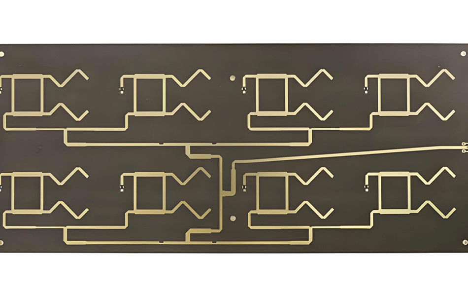
The industry uses four terms loosely and they set different requirements. RF spans the whole 3 kHz to 300 GHz range as a general term. A high-frequency board denotes a material class with controlled Dk and low Df. Microwave conventionally starts at about 1 GHz, where the guided wavelength drops below a few hundred millimetres and distributed effects replace lumped ones. Millimetre wave begins at 30 GHz, where the guided wavelength falls under about 10 mm and mechanical tolerance starts to be measured in fractions of a wavelength.
The reason the 1 GHz line matters is geometric. Anything longer than about one twentieth of the guided wavelength behaves as a transmission line and reflects; anything shorter than that can usually be treated as a lumped element. On a Dk 3.38 microstrip the effective Dk is about 2.67, so the guided wavelength is 300 mm at 1 GHz, 30 mm at 10 GHz and 3.9 mm at 77 GHz. Divided by twenty, the threshold for “this feature is now electrical” falls from 15 mm to 1.5 mm to 0.2 mm across that range.
| Frequency | Free-space λ0 | Guided λg, Dk 3.38 (εeff 2.67) | Guided λg, 5880 (εeff 1.87) | Feature size that starts to matter (λ/20) |
|---|---|---|---|---|
| 1 GHz | 300 mm | 184 mm | 219 mm | 9–11 mm |
| 3 GHz | 100 mm | 61 mm | 73 mm | 3.1–3.7 mm |
| 10 GHz | 30 mm | 18.4 mm | 21.9 mm | 0.9–1.1 mm |
| 24 GHz | 12.5 mm | 7.7 mm | 9.1 mm | 0.38–0.46 mm |
| 40 GHz | 7.5 mm | 4.6 mm | 5.5 mm | 0.23–0.27 mm |
| 77 GHz | 3.9 mm | 2.4 mm | 2.9 mm | 0.12–0.14 mm |
Read the last column as a tolerance specification. At 77 GHz, a 0.12 mm feature is electrically visible; a drill position error of 25 µm is a fifth of that, and a laminate thickness error of 25 µm is the same. Nothing in the process is difficult at 1 GHz and almost everything is difficult at 77 GHz, which is why a microwave job has to be quoted and routed against a frequency rather than against a layer count.
Dielectric loss follows αd ≈ 2.6 · fGHz · √Dk · Df. At 10 GHz, RO4003C with Df 0.0027 costs 0.13 dB/in, RO3003 with 0.0010 costs 0.045 dB/in, and RT/duroid 5880 with 0.0009 costs 0.035 dB/in. The gap between the hydrocarbon grades and the PTFE grades is roughly a factor of three, and it widens with frequency because the expression is linear in f.
| Laminate | Dk | Df | TCDk | Water absorption | What it means on a microwave board |
|---|---|---|---|---|---|
| RO4350B | 3.48 | 0.0037 | +50 ppm/°C | 0.06 % | Cheapest route to controlled impedance, hybrid with FR-4; Df limits it above about 10 GHz |
| RO4003C | 3.38 | 0.0027 | +40 ppm/°C | 0.06 % | The default for 8–20 GHz; stable Dk over temperature, good dimensional control |
| RO3003 | 3.00 | 0.0010 | −3 ppm/°C | 0.04 % | No glass, so no weave effect; Dk nearly flat with temperature |
| RT/duroid 5880 | 2.20 | 0.0009 | −125 ppm/°C | 0.02 % | Lowest loss, but the Dk drifts with temperature and the Z-axis CTE is 237 ppm/°C |
| Taconic TLY-5 | 2.20 | 0.0009 | about −120 ppm/°C | 0.02 % | Same design point as 5880; a second source, not a different trade |
| Taconic RF-30 | 3.00 | 0.0014 (at 1.9 GHz) | not published; assumes PTFE-like drift | 0.04 % | Sits between 3003 and 4003C on loss, at a lower price |
The column that decides phase-critical work is TCDk, not Df. A 5880 design at −125 ppm/°C changes Dk by about 1.2 % over a 100 °C excursion, which moves both impedance and electrical length; a 4003C design moves by about 0.4 % in the opposite direction. In a phased array that difference is a phase error that has to be calibrated out at every temperature, and in a filter it is a passband that walks. Neither effect appears in a room-temperature coupon measurement, which is why the temperature coefficient belongs in the material specification rather than in the appendix.
Material selection for microwave work is therefore a three-variable problem: loss at the operating frequency, Dk stability over the operating temperature range, and mechanical behaviour at the layer count required. The comparison in material selection for microwave PCB manufacturing walks through the same trade from the supply side; the property tables behind the numbers are in high-frequency microwave PCB materials and their properties.
Skin depth in copper falls as 2.06/√f µm, so 0.65 µm at 10 GHz becomes 0.46 µm at 20 GHz, 0.33 µm at 40 GHz and 0.24 µm at 77 GHz. Against a standard electrodeposited foil with 2.5–3 µm rms roughness, the current path at 40 GHz is an order of magnitude longer than the geometry suggests.
| Frequency | Skin depth, copper | Skin depth, nickel | Roughness factor, standard ED foil | Roughness factor, HVLP foil |
|---|---|---|---|---|
| 1 GHz | 2.06 µm | 4.20 µm | about 1.2 | about 1.05 |
| 10 GHz | 0.65 µm | 1.33 µm | about 1.9 | about 1.45 |
| 20 GHz | 0.46 µm | 0.94 µm | about 1.95 | about 1.6 |
| 40 GHz | 0.33 µm | 0.66 µm | about 1.98 | about 1.75 |
| 77 GHz | 0.24 µm | 0.48 µm | about 2.0 | about 1.85 |
Two readings follow. The roughness penalty saturates rather than grows, because once the roughness is many times the skin depth the current has already taken the long way round; what grows is the total copper loss, since copper loss itself rises as √f. And the nickel column explains the finish problem: at 40 GHz a 3–6 µm ENIG nickel layer is ten times the skin depth, so the current runs entirely in a metal with roughly four times the resistivity of copper, and the launch loss stops being a rounding error.
The production consequence is that foil and finish have to be specified together. Buying an HVLP foil and then finishing with ENIG is spending money twice and removing most of the benefit; buying standard foil and finishing with OSP leaves the roughness penalty in place. Foil by foil, the difference between electrodeposited and rolled annealed copper is set out in the guide to PCB copper foils.
On a 0.254 mm 5880 stack at 10 GHz, the guided wavelength is 21.9 mm. A dielectric thickness error of ±10 %, which is the standard laminate tolerance, moves the impedance by about ±6 % and the electrical length by about ±5 % at the same time. In a phase-matched pair that second effect is the one that hurts: two lines of equal physical length but different dielectric thickness no longer have equal delay.
PTFE adds a failure mode that epoxy laminates do not have. The material cold-flows under lamination pressure, so the finished thickness is a function of press cycle rather than of the incoming sheet. A 4 % compression takes a 50 Ω line to 48.8 Ω — small in isolation, but it arrives as a systematic offset across the whole panel rather than as random scatter, and it is not visible in any incoming inspection. This is why PTFE stacks use thicker dielectric than the electrical design strictly needs, and why 0.127 mm cores are treated with suspicion on microwave work.
The design response is to keep the electrical design tolerant of the thickness it will actually get: pick a stack where ±10 % thickness leaves the impedance inside the window quoted to the customer, and state the impedance window on the drawing rather than assuming ±10 % everywhere. The arithmetic for both is in high-frequency PCB stack-up design.
Microwave multilayers are usually PTFE cores bonded with a thermoplastic film or a low-flow prepreg. The film is not a mechanical accessory: it is a dielectric layer in the stack, with its own Dk and its own thickness, and leaving it out of the field solver is the classic way to produce a board that is 20 % high in impedance.
| Bonding route | Bond temperature | Typical thickness | Implication for the stack |
|---|---|---|---|
| FEP film | 290–315 °C | 0.038–0.10 mm | Lowest loss; needs a dedicated high-temperature press cycle and a slow ramp |
| Low-flow PTFE-compatible prepreg | 180–190 °C | 0.05–0.10 mm | Allows a lower cycle but adds a lossy layer between cores that must be in the impedance model |
| Hydrocarbon prepreg (for 4000 series) | 190–200 °C | 0.05–0.15 mm | Bonds 4350B to FR-4; Df around 0.004, so it sets the loss floor of a hybrid |
| FR-4 prepreg (hybrid only) | 170–190 °C | 0.10–0.20 mm | Cheap, but Df 0.016–0.025 makes it unusable inside a microwave field region |
Three production rules follow from the table. First, the press cycle is set by the highest-temperature material in the stack, not by the majority material, so a single FEP layer forces the whole build to 290 °C and that in turn constrains which inner layers can already be imaged. Second, each bonding layer has to be present in the impedance model with its own thickness and Dk; a 0.10 mm film that is omitted moves a 50 Ω line to 61 Ω. Third, the film flows, which means the finished dielectric thickness under a large copper pour differs from the thickness under a sparse area — the same panel can then hold two different impedances.
Lamination windows, ramp rates and the pressure profile are covered station by station in lamination in high-frequency PCB manufacturing; the microwave-specific point is simply that the film, not the core, is what usually ruins a first article.
PTFE does not machine like epoxy. It is soft, it has a low melting point relative to the drilling temperature at the tool edge, and it does not absorb the chemistry that removes epoxy smear. The result is a hole with a burr at the exit, a smear that permanganate cannot touch, and a wall that no aqueous chemistry will wet.
| Step | Epoxy laminate | PTFE laminate | Number that changes |
|---|---|---|---|
| Desmear | Permanganate, 3–5 min swell + 10–15 min | Sodium naphthalenide or plasma only | Barrel connectivity: a 10 % void is a field failure, not a cosmetic defect |
| Maximum aspect ratio | 8:1 to 10:1 | about 6:1 | Throw into a non-wetting wall |
| Drill bit life | 2,000–3,000 hits | 500–1,000 hits | Burr height grows with wear before hole size does |
| Entry / exit material | Standard aluminium entry | Aluminium entry, backing board mandatory | Exit burr on PTFE is the usual cause of a short after assembly |
| Z expansion at reflow | 17–24 µm for 1.6 mm FR-4 | about 82 µm for 5880 | The barrel has to stretch, so plating elongation ≥20 % |
The aspect ratio ceiling of 6:1 is sometimes presented as a manufacturer preference. It is not: it is the point beyond which the combination of a non-wetting wall, a 237 ppm/°C Z expansion and a 20 µm-thick plating cannot be made to survive thermal cycling. On a 1.6 mm board that puts the practical hole diameter floor at about 0.27 mm, which is a design constraint that has to be known before the stack is drawn. Drill parameters specifically for 5880 are worked through in RO5880 drilling parameter optimisation.
A plated through hole that passes through a signal layer and continues to the bottom of the board leaves an open-circuited stub. The stub resonates at f = c/(4L√εeff), and below that resonance it presents a capacitive discontinuity that grows with frequency. On a microwave board the stub length is often set by the mechanical thickness, so the resonance arrives at a frequency nobody chose.
| Stub length | FR-4 (εeff 4.2) | 4350B (εr 3.48, stripline) | 5880 (εr 2.20, stripline) |
|---|---|---|---|
| 2.4 mm through | 15.3 GHz | 16.7 GHz | 21.1 GHz |
| 1.6 mm through | 22.9 GHz | 25.1 GHz | 31.6 GHz |
| 0.9 mm blind | 40.8 GHz | 44.6 GHz | 56.2 GHz |
| 0.08 mm microvia | 459 GHz | 501 GHz | 632 GHz |
The table explains a pattern that surprises designers new to microwave work: moving from FR-4 to PTFE raises the stub resonance, because the lower Dk makes the stub electrically shorter. The improvement is 35–40 % for the same physical length — helpful, but never enough to rescue a 2.4 mm through-hole at 24 GHz. The only real fixes are back-drilling, blind and buried vias, or routing the signal on the layer that makes the stub as short as possible. Back-drilling has its own tolerance: a 0.2 mm depth error shifts the resonance by roughly 2 % and leaves a stub that is short but not absent, which is why drilling is a microwave design decision rather than a fabrication detail.
Grounded coplanar waveguide is the standard transmission line on a microwave board because it keeps the field close to the surface and tolerates a thinner substrate. Its weakness is that the impedance depends on a gap that is often narrower than the trace, and a narrow feature is where tolerance hurts most.
Take a GCPW on 0.254 mm 5880 with a 0.50 mm centre conductor and a 0.25 mm gap. A ±25 µm etch error is ±10 % of the gap and about ±5 % of the centre width. In a field solve for this geometry the centre width dominates: a 10 % change in centre width moves the impedance by roughly four times as much as a 10 % change in gap. The practical conclusion is counter-intuitive — the gap can be left slightly loose, but the centre conductor cannot, and the etch compensation should be applied to the trace and not to the gap.
The second coplanar issue is the mask. A solder mask bridge across a 0.25 mm gap fills it with a dielectric of Dk 3.5–4.5 and changes the effective permittivity of the region where the field is concentrated. On a 0.5 mm centre line the shift is a couple of ohms; on a 0.2 mm line it is more. Opening the mask over the gap is free in the artwork and is the single cheapest microwave improvement available at the design stage.
PTFE absorbs very little water — 0.02 % for 5880 and TLY-5, 0.04 % for 3003, against 0.06 % for the hydrocarbon grades and considerably more for FR-4. That is often read as “no baking needed”. The mistake is that the cores are not the only hygroscopic part of the stack: the bonding film, the prepreg and the FR-4 layers in a hybrid all absorb, and they all release at press temperature.
Trapped moisture produces two specific defects. It expands at the press or reflow temperature and shows up as blistering or as a measured thickness increase after the first thermal cycle, both of which move the impedance. And it produces a dimensional change: a panel that has absorbed water is slightly larger than a dry one, so artwork compensation derived from a wet panel is wrong by the amount the panel shrinks on drying.
The process answer is a bake before lamination, typically 4 hours at 120 °C for PTFE builds and longer for hybrids with FR-4 layers, followed by a controlled cool-down and a defined hold time before pressing. The design answer is a stack whose impedance window can absorb a 1–2 % thickness change without going out of specification.
On a microwave board the finish is part of the transmission line for the length of the launch and for every exposed filter feature. The comparison is set by the skin depth column earlier: at 20 GHz, 0.94 µm in nickel against 0.46 µm in copper. A 3–6 µm ENIG nickel layer is several skin depths thick, so the current is carried in nickel and the surface resistance rises by roughly a factor of two.
Practically: OSP where the assembly window allows it, immersion silver where shelf life matters, ENIG where wire bonding or fine pitch forces it, and never hard gold on a transmission line. The finish comparison, including the thickness windows that IPC specifies, is in PCB surface treatment processes. One microwave-specific addition: whatever the finish, the copper underneath has to be free of oxide and of resist residue, because a 0.1 µm interfacial layer is a meaningful fraction of the skin depth at 40 GHz.
A microwave coupon has to resemble the product in three respects: the same stack, the same launch, and the same reference-plane spacing. A coupon measured with a different transition measures the transition, not the line.
| Method | Useful range | What it gives | What it misses |
|---|---|---|---|
| TDR, 35 ps edge | DC to about 10 GHz equivalent | Impedance profile, discontinuity location | Loss, and any feature shorter than about 3.5 mm |
| VNA with SOL calibration | 10 MHz to 40 GHz | Insertion and return loss, group delay | Calibration kit errors dominate above 26 GHz |
| VNA with TRL calibration | Band-limited, per waveguide band | Loss to a few tenths of a dB | Needs a purpose-built calibration set per band |
| Resonator (split-post / cavity) | Single frequency per fixture | Dk and Df of the laminate itself | Nothing about the manufactured line |
The calibration question is where microwave testing usually fails on paper. A SOL kit calibrated at the connector plane leaves the launch inside the measurement; a TRL set moves the reference plane to the coupon and is the only way to see a 0.1 dB difference between two laminates. If the customer needs a loss number rather than an impedance number, the test method has to be agreed before the coupon is drawn, not after the boards are shipped. The wider set of test criteria is in key points during high-frequency PCB testing.
PTFE is soft enough that ordinary panel handling shows up electrically. V-scoring a 0.5 mm PTFE panel produces a stress concentration at the score line, and the delamination that follows is often attributed to lamination. Routing is preferred, with a 2 mm minimum web between boards. Panel bow is another: a 0.254 mm 5880 core on a 300 mm span bows visibly under its own weight at reflow temperature, and the coplanarity matters if the board sits in a metal housing with a defined cavity depth.
For cavity-backed designs the machining tolerance of the housing is part of the electrical stack. A cavity depth tolerance of ±25 µm on a 0.254 mm substrate is a 10 % change in the air gap, which shifts the resonant frequency of a patch by roughly the same percentage. That is why microwave mechanical drawings carry the cavity tolerance in micrometres alongside the laminate thickness, and why the laminate and the housing are usually qualified together rather than separately.
The defects that kill a microwave build are rarely the ones the visual inspection catches. Four account for most of the losses, and each has a detectable signature if the process is set up to look for it.
| Failure mode | Threshold that matters | How it is caught |
|---|---|---|
| Layer-to-layer slip during press | >25 µm on a 77 GHz design | X-ray of a dedicated registration target, first article and sampling |
| Barrel void after desmear | >10 % of wall area | Cross-section after 3× thermal shock; continuity testing will not see it |
| Bonding-film void or thickness loss | >10 µm, or a void over a ground plane | C-SAM or cross-section; impedance reads low locally |
| Impedance out of window | ±5 % at 20 GHz and above | Coupon at the panel centre and edge, both measured |
| Burr at the hole exit | >25 µm | Optical inspection after drilling, before plating |
The common factor is that all five are process-capability failures rather than workmanship failures, so they are prevented by the first article and the sampling plan rather than by operator attention. That is the difference between a microwave job and a standard multilayer job: the standard job can be inspected into quality, the microwave job has to be designed and qualified into it.
The list of considerations for a microwave board is short once it is expressed physically. Guided wavelength sets which geometry becomes electrical, from 9 mm at 1 GHz down to 0.12 mm at 77 GHz. Skin depth sets which metal carries the current, from 2.06 µm at 1 GHz to 0.24 µm at 77 GHz, and therefore why foil roughness and finish thickness stop being cosmetic. Stub resonance sets the via policy, and it moves by 35–40 % simply by changing the laminate. Thickness tolerance sets both impedance and electrical length, and PTFE adds a cold-flow term that epoxy does not have. The bonding film is a dielectric in the stack, not an adhesive under it.
Everything else — the press cycle, the desmear chemistry, the drill bit life, the bake, the coupon — follows from those five. A microwave job that is reviewed against them is a job with predictable yield. A job that is reviewed against a high-frequency checklist is a job that will pass its prototype and disappoint in volume.
XCE PCB builds microwave multilayer on PTFE and hydrocarbon laminates: 2 to 72 layers, 600×1200 mm panels, impedance held to ±10 %, sodium naphthalenide and plasma desmear lines, samples in as fast as 24 hours, inspected to IPC-A-600G and IPC-6015. The production decisions that precede this stage are set out in considerations in the production process of high-frequency PCB, and the station-by-station windows in the production process of high-frequency PCBs.
Send us your Gerber files and requirements for a manufacturability review and a tailored quotation.