
The standard introduction and function of single-sided and multi-layer PCBs is written as a list of adjectives: single-sided is cheap and simple, multi-layer is dense and has good signal integrity. None of that explains why the second board costs three times as much, and one of those adjectives is wrong in a way that misleads design teams. The function a multi-layer board adds is not more routing, and certainly not a layer count. It is a reference plane: a continuous return path a fixed distance from every signal. Everything else — impedance you can control, crosstalk you can predict, radiation you can suppress — follows from that one geometric fact. This article defines both boards by what they can and cannot do, then gives the criterion that decides between them: edge length against trace length, not frequency against a spec sheet.
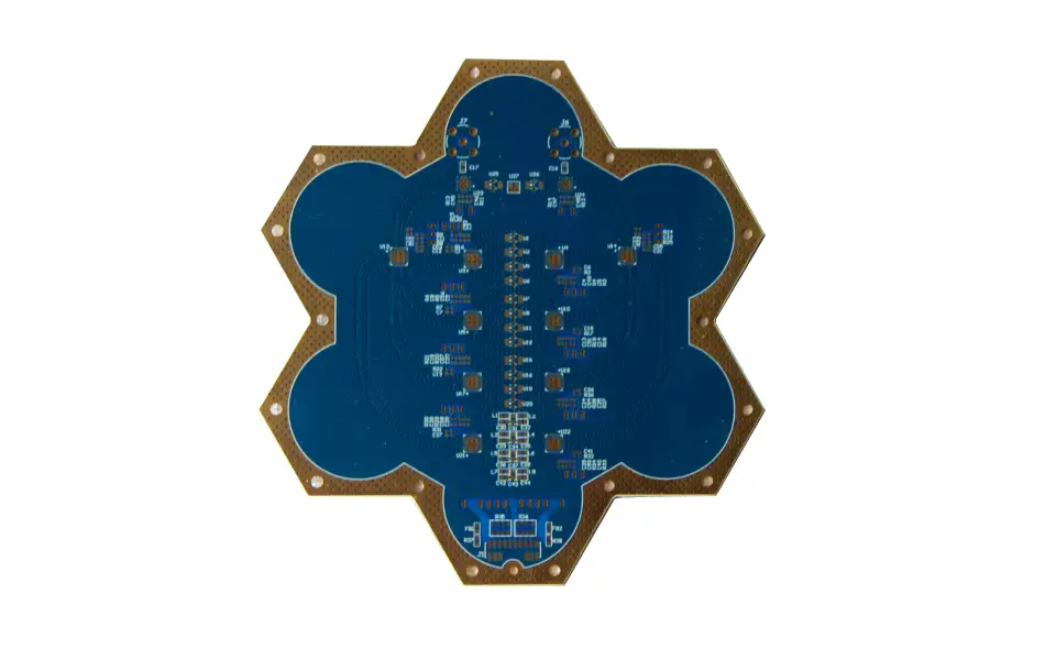
The Layer Count Is Not the Function
A single-sided board has one copper layer on one face, a dielectric beneath it, and holes that are mechanical rather than plated. A multi-layer board has three or more conductor layers separated by dielectric and joined by plated vias. Those are the definitions, and they are settled. What is not settled in most introductions is the function question: what does the second, third and fourth layer actually do that the first one cannot?
Three things, and only the first one is electrical:
| Function | Mechanism | What it replaces on a single-sided board |
|---|---|---|
| Reference plane | A continuous copper plane at a fixed distance from the signal, so the return current has a defined path and the field is confined | A return that finds its own way along neighbouring traces and board edges |
| Vertical routing | Inner layers carry traces and planes that would otherwise compete for the same face | Every net on one face, so density is set by the face area |
| Mechanical | Symmetric stacks control warp; internal planes act as shields and as heat spreaders | Thickness and flatness set by the base material alone |
The electrical column is the one that decides most designs, and it is the one usually described in the wrong direction. Multi-layer boards do not have better signal integrity because they have more layers. They have better signal integrity because one of those layers is a plane, and a plane turns an uncontrolled wire into a transmission line with a defined impedance and a return path of known width.
What a Single-Sided Board Is, Structurally
Four elements, and the thickness of each is a specification rather than a default.
| Element | Typical range | What it controls |
|---|---|---|
| Copper foil | 1 oz (35 µm) standard, 2 oz for power | Current capacity, minimum etchable width |
| Laminate | 0.8 mm, 1.0 mm, 1.6 mm paper- or glass-based phenolic, or FR-4 | Mechanical stiffness, Dk, cost |
| Solder mask | 15–25 µm | Solder bridging, surface insulation resistance |
| Finish | HASL or OSP in most cases, ENIG where flatness matters | Shelf life, solderability, cost |
The structural detail that matters most and is almost never stated: on a single-sided board the component holes are usually not plated. The lead passes through a drilled or punched hole and is soldered on the copper side, so the hole is a mechanical feature with no barrel, no annular ring requirement and no plating thickness — the contrast with a plated barrel is set out in PCB through hole. That is why single-sided boards are so cheap — there is no electroless copper line, no panel plating and no hole-wall inspection in the flow — and it is also why nothing on a single-sided board can be connected from the back.
Etching has the same trapezoid problem as on any other board, and with no plating afterwards it is the only thing setting width. At an etch factor of 1.5, 1 oz foil undercuts about 23 µm per side, so a 0.2 mm drawn line finishes near 0.15 mm at the base. That is why the practical minimum on a single-sided board is about 0.2 mm rather than the 0.1 mm quoted for a plated inner layer, an asymmetry explained in PCB etching.
Three Things a Single-Sided Board Cannot Do
It cannot control impedance. Characteristic impedance is a property of a conductor and its return reference. With no plane, the “reference” is whatever copper happens to be nearby — a neighbouring trace, a ground track along the edge, a component lead — so the impedance varies from millimetre to millimetre and cannot be designed or measured against a coupon.
It cannot confine the field. On a board with a plane 0.2 mm below the trace, the return current flows directly underneath and the loop area for a 50 mm trace is about 10 mm². On a single-sided board the same trace may have its return 2–5 mm away in the plane of the board, so the loop area is 100–250 mm². Radiated emission scales with loop area, so the difference is 20–28 dB before any discussion of what the traces are doing.
It cannot predict crosstalk. With no plane, the field spreads through the dielectric and through the air on the component side, and it reaches neighbours that a plane would have screened. Measured side-by-side comparisons at the same spacing typically show 10–20 dB more near-end crosstalk on the board without a reference plane, and the number moves with whatever else is routed nearby, which is the real problem: it is not repeatable.
| Property | Single-sided | With one reference plane | Ratio |
|---|---|---|---|
| Return path | Undefined; nearest copper | Directly under the trace | — |
| Loop area, 50 mm trace | 100–250 mm² | About 10 mm² | 10–25× |
| Impedance tolerance | Not specified | Designable, ±10 % typical | — |
| Crosstalk at fixed spacing | Baseline | 10–20 dB lower | 10–100× in voltage |
| Coupon measurement possible | No | Yes, TDR or VNA | — |
The Real Criterion Is Edge Length, Not Frequency
The question “can this run at 100 MHz on a single-sided board” has no answer, because a 100 MHz sine wave and a 100 MHz clock with a 1 ns edge are different electrical objects. What decides whether a trace behaves as a wire or as a transmission line is the ratio of the signal’s rise time to the time it takes to travel the trace.
Propagation delay on an FR-4 microstrip with an effective Dk around 3.3 is about 6.1 ns/m, or 154 ps/inch. The classic threshold is a flight time of half the rise time; conservative design guides use a sixth.
| Rise time | Critical length at tflight = tr/2 | Conservative at tr/6 | What that means in practice |
|---|---|---|---|
| 10 ns | 820 mm | 270 mm | Single-sided is fine for almost any board this size |
| 2 ns | 165 mm | 55 mm | Fine until the board grows past a business card |
| 1 ns | 82 mm | 27 mm | The boundary; most controllers are here |
| 300 ps | 25 mm | 8 mm | Needs a plane for anything longer than a package escape |
| 100 ps | 8 mm | 2.7 mm | Single-sided is not an option |
Read the table as a design rule rather than a limit. A single-sided board with a 1 ns driver and 60 mm of trace is at the boundary: it will work in the lab and fail EMC, or work at room temperature and ring at 85 °C when the driver slows. The reason is not that the board is single-sided; it is that the return current has to find a path, and at that edge rate the path it finds is a loop antenna.
Wavelength gives the same answer in the frequency domain. On the same laminate the guided wavelength is 1.65 m at 100 MHz, 165 mm at 1 GHz and 16.5 mm at 10 GHz, so a 50 mm trace is λ/33 at 100 MHz and λ/3 at 1 GHz. Phase, delay and coupling all become layout-dependent somewhere between those two.
Why Four Layers Is the First Useful Number
Layers are not added one at a time. They are added in pairs, because a stack has to be symmetric to stay flat, and the useful configurations are set by a simple counting rule: a stripline needs a plane above and below, so n stripline layers need at least n+1 planes.
| Layer count | Usable arrangement | What it enables | What it still cannot do |
|---|---|---|---|
| 1 | One copper face | Mechanical holes, simple nets, low edge rates | No plane, no controlled impedance |
| 2 | Copper both faces | Crossovers, a ground pour on the second face | The pour is interrupted by traces, so the return path breaks |
| 4 | Signal / plane / plane / signal | Two microstrip layers with a solid reference each | No stripline; inner layers are planes, not routing |
| 6 | Signal / plane / signal / signal / plane / signal | Two microstrip and two inner layers, one of them stripline-capable | Inner signal layers adjacent to each other couple |
| 8 | Signal / plane / signal / plane / plane / signal / plane / signal | Multiple stripline layers, controlled impedance everywhere | Cost, press cycles, registration budget |
That is why the four-layer board is the first one that is electrically different rather than merely denser: it is the first one where every signal can see a continuous plane. It is also why a two-layer board with a ground pour is not a substitute: the pour is perforated by the very traces it is supposed to reference, and the return current has to detour around every one of those perforations, which is where the loop area in the previous section comes from.
The layer-by-layer construction, and the rule that the stack is derived from the planes rather than from the routing, is set out in PCB layer structure and in high-frequency PCB stack-up design.
What Each Extra Layer Costs
Cost is not linear in layer count, and the reason is that each pair of layers adds a press cycle, an inner-layer imaging step, an AOI step and a registration risk.
| Construction | Relative cost (single-sided = 1) | Main driver |
|---|---|---|
| Single-sided, 1.6 mm FR-4 | 1.0 | Material and one imaging step |
| Double-sided, plated | 1.6–2.0 | Adds electroless copper, plating, hole-wall inspection |
| 4-layer | 2.5–3.5 | Adds inner imaging, oxide, one press cycle |
| 6-layer | 3.5–4.5 | Second press cycle, tighter registration, lower yield |
| 8-layer | 5.0–7.0 | Three press cycles, aspect ratio, test time |
The table is a ratio, not a price, and it moves with panel utilisation, hole count and material. What it shows is the shape of the decision: going from one layer to four roughly triples the board cost, and going from four to eight roughly doubles it again. A design that adds four layers to save 200 mm² of board area is usually making a bad trade unless the enclosure is the binding constraint.
Can a Single-Sided Board Carry High Frequency?
Yes, within limits that are set by geometry rather than by the word “high frequency”. A coplanar waveguide — a signal trace with ground tracks either side on the same face — gives a defined impedance without a back-side plane, and single-sided CPW filters and antenna feeds are common below about 6 GHz on low-cost substrates.
The costs are specific. The ground tracks have to be wide enough and stitched often enough that they behave as one conductor, and on a single-sided board there is no second face to stitch to, so the “ground” is a set of tracks whose inductance depends on how far apart the stitching points are. Radiation loss rises because the field is not confined to one side of the board, and the effective Dk sits between the substrate and air, which makes the impedance sensitive to conformal coating, enclosure proximity and even humidity.
Above roughly 10 GHz the balance tips: the wavelength on the board is 16.5 mm, a transition or a bend is a measurable discontinuity, and there is no plane to reference the return. At that point the board is not “single-sided high frequency”, it is a mechanical carrier with an antenna on it, and the RF laminate decision has already moved the design to a multilayer stack.
Five Claims That Do Not Survive
The original article, like most introductions, contains statements that read well and fail on inspection. Five of them:
| Claim | What is actually true |
|---|---|
| Multi-layer boards have better signal integrity because they have more layers | Because they have a plane. Ten signal layers with no continuous reference are worse than four layers with two solid planes |
| Multi-layer boards are more flexible in shape | The opposite. Each press cycle adds registration tolerance and warp risk; complex outlines, thin sections and rigid-flex transitions get harder with layer count, not easier |
| More layers help dissipate heat | Only if the planes are thermally connected to the heat source with vias. A copper plane separated from a component by 0.2 mm of a laminate with 0.2–0.3 W/m·K is 8–13 K/W per cm² of thermal resistance |
| Single-sided boards are only for low frequency | They are limited by edge rate and trace length. A 10 ns microcontroller runs happily on a single-sided board at 100 MHz; a 100 ps SerDes does not run on a plane-less board at any frequency |
| Multi-layer is always the better engineering choice | It is a cost trade. Where the edge length criterion in section 4 is met, the plane buys nothing and the money is better spent on the laminate or the finish |
How the Two Are Made, and How They Are Checked
The flow difference is the reason for the cost difference, and it is a difference in kind rather than in effort.
| Stage | Single-sided | Multi-layer |
|---|---|---|
| Cutting | Yes | Yes |
| Drilling | Mechanical holes, unplated | Plated through, blind or buried |
| Inner imaging | None | Per inner layer, with AOI |
| Bonding | None | Oxide plus one press per pair |
| Plating | None | Electroless copper plus pattern plate |
| Electrical test | Continuity and isolation | Netlist test, plus coupon impedance |
| Typical acceptance | IPC-A-600 Class 2 | IPC-6012 Class 2 or 3, plus IPC-6015 where applicable |
The practical consequence for a buyer is that a single-sided quote is dominated by material and tooling, while a multi-layer quote is dominated by process steps and yield. That is why the same outline can be quoted at three very different prices by shops with the same material cost: what differs is the number of press cycles they are willing to run and the impedance verification they include. The twelve steps behind that quote are mapped in high-frequency PCB manufacturing process.
A Five-Question Decision Path
Five questions, in this order, settle the choice for most boards:
1. What is the shortest edge in the design, and how long is the longest trace it drives? If the trace is shorter than tr/2 in flight time — 82 mm at 1 ns — a plane buys little. 2. Does anything need a controlled impedance? If yes, a plane is mandatory and the board is at least four layers. 3. Is there a compliance requirement? Radiated emission limits are usually what forces the plane on an otherwise marginal design. 4. How many nets have to cross each other? Crossovers, not component count, drive the layer count. 5. What does the enclosure allow? A 4-layer board is thicker and heavier than a 1.6 mm single-sided one, and in a handheld product that can be the binding constraint.
Answer those five and the layer count is usually obvious. What is left is the choice within a family — single-layer, multilayer or high-layer-count with blind and buried vias — which is a question of density and via strategy rather than of electrical function, and it is covered in multilayer versus single-layer high-frequency PCBs.
Conclusion
A single-sided board is one copper face with unplated holes; a multi-layer board is three or more conductor layers with plated connections. The function that the extra layers add is a reference plane, and from that plane come controlled impedance, a confined field, predictable crosstalk and measurable coupons. The layer count is a consequence, not the cause: four layers is the first configuration where every signal can see a continuous plane, and eight is where a proper stripline stack becomes economic.
The criterion for choosing between them is measurable and has nothing to do with a frequency printed on a datasheet. Compare the rise time to the flight time: 6.1 ns/m on FR-4 means a 1 ns edge is critical at 82 mm, a 300 ps edge at 25 mm and a 100 ps edge at 8 mm. Below those lengths a plane is a luxury; above them it is the only way to know what the trace impedance is.
XCE PCB builds both ends of that range: single- and double-sided boards for control and power, and high-frequency multilayer stacks from 4 to 72 layers on 600×1200 mm panels, impedance held to ±10 % with coupon verification, samples in as fast as 24 hours, inspected to IPC-A-600G and IPC-6015. If the edge-rate calculation lands near a boundary, send the stack and we will quote both — request a quote or WhatsApp +86 180 3818 8537.
Frequently Asked Questions
What is the main functional difference between single-sided and multi-layer PCBs?
Is a two-layer board with a ground pour as good as a four-layer board?
How do I know whether my design needs a plane?
Can high-frequency circuits run on a single-sided board?
Are the holes on a single-sided board plated?
Does adding layers improve heat dissipation?
From Single-Sided Prototypes to 72-Layer Builds
Send us your Gerber files and requirements for a manufacturability review and a tailored quotation.
sales1@xcepcb.com
+86 180 3818 8537