
Every article about HDI manufacturing difficulties contains the same headings — microvia drilling, thin lines, lamination, surface finish, inspection — and almost none of them contains a number, which is why the earlier version of this page ended with an invented case study claiming 98 % yield and a 20 % reduction in production time. The challenges are real, but they arrive in four accounts: an error budget that compounds with every press cycle, a fill specification that decides whether a via survives assembly, a warpage figure that decides whether the board can be assembled at all, and an inspection capability that cannot see most of the three. This article works through the four, then through scrap attribution, equipment auditing and the arithmetic that turns yield into price.
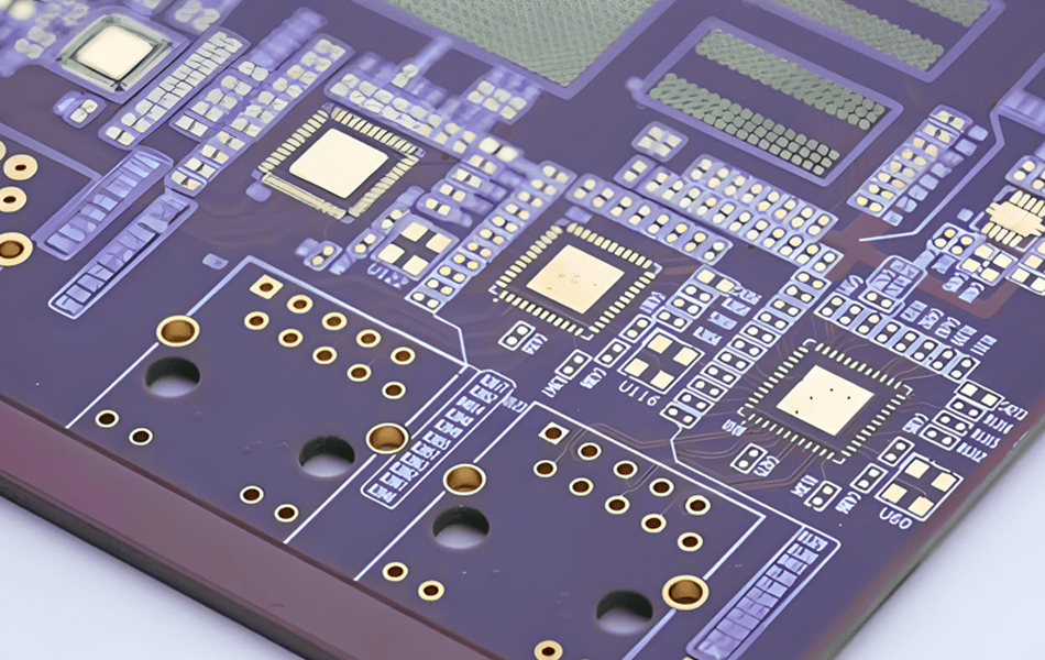
A list of challenges is unfalsifiable; a ledger has a column for the number. HDI difficulties reduce to four quantities, and each is measurable before, during and after production. Registration error is accumulated position error between layers, in micrometres, and it compounds with the number of press cycles. Via fill is a void fraction and a dimple depth, in percent and micrometres. Warpage is a percentage of diagonal after a stated thermal excursion. Inspection is a capability: a resolution in micrometres and, more importantly, a list of defects it cannot see.
| Ledger | The number | Where it fails | Who pays for it |
|---|---|---|---|
| Registration | ±25 µm per lamination cycle | Capture land on stacked microvias, through-via annular ring | Design, at layout; factory, at press |
| Via fill | Void <2 %, dimple ≤25 µm | Via-in-pad: solder wicking, blowholes, head-in-pillow | Factory, at fill and planarisation |
| Warpage | 0.2–0.3 % of diagonal after 260 °C | Placement, paste printing, coplanarity of a BGA | Both: stack symmetry is a design choice |
| Inspection | Optical 25 µm; X-ray for voids | The three above, most of the time | Nobody, until the field |
The fourth row is the one that makes HDI different from conventional PCB manufacturing. On a conventional board the inspection gates largely confirm what the process already controls; on HDI the defects that matter — a void under a filled via, a partially opened capture land, a 20 µm delamination between build-up layers — are either invisible to the standard gates or visible only destructively.
Each lamination cycle aligns the new layer to targets drilled in the existing panel. The alignment itself is good — a CCD or X-ray target system holds ±10–15 µm — but the error is per cycle and, for a stacked column, all cycles apply to the same axis. Two cycles give a worst case of ±50 µm; four give ±100 µm, even if the statistical sum is smaller.
The arithmetic meets the geometry in the capture land. A 100 µm microvia in a 250 µm land has 75 µm of copper on each side at nominal. At ±50 µm of accumulated error, 25 µm remains — enough to plate, not enough to be comfortable. At ±75 µm the via breaks out of the land and the connection is a crescent, which passes continuity and fails thermal cycling.
Three controls are effective and they act at different stages. In design: stagger instead of stack wherever the land allows, because staggering gives each layer its own independent target. In CAM: compensate the capture land for the number of cycles, rather than using one land size for every build-up layer. In production: measure the actual registration per layer on a test coupon and stop the lot when the accumulated figure approaches the design margin — the process windows that produce those figures are set out in HDI PCB manufacturing process.
Via-in-pad requires the via to be filled, cured, planarised and plated over, so that the pad is flat enough to print paste onto. The two numbers that define “flat enough” are the void fraction after cure and the dimple after planarisation: voids under 2 % of the via cross-section are the usual acceptance limit, and dimple of 25 µm or less is what keeps paste volume predictable at 0.4 mm pitch.
| Defect | How it is created | What it does later | Limit and detection |
|---|---|---|---|
| Void in the fill | Air trapped during paste fill, or outgassing during cure | Blowhole through the pad during reflow; solder wicking into the via | Under 2 % area; X-ray, not AOI |
| Dimple | Incomplete planarisation, or fill shrinkage on cure | Low paste volume, leading to a weak joint; coplanarity failure at fine pitch | 25 µm; profilometer on a coupon |
| Fill pull-out | Poor adhesion between fill and barrel, or thermal shock | Open after thermal cycling | Cross-section; thermal cycle test |
| Plating over the fill | Resin smear on the fill before plating | Pad delamination at reflow | Cross-section and peel test |
The commercial consequence is that fill quality is a factory capability rather than a design parameter, and it is one of the few HDI capabilities that can be audited from documentation: ask for the void and dimple acceptance limits, the inspection method for each, and the coupon on which they are measured. A supplier who states only “via-in-pad available” has not stated a capability.
Warpage on thin HDI is dominated by three asymmetries: copper distribution between the two sides, the number of build-up layers on each side, and the difference in thermal expansion between the core and the build-up films. A 0.2–0.3 % figure of diagonal after a 260 °C excursion is the practical acceptance band for a thin board; on a 150 mm panel diagonal that is 0.3–0.45 mm, which is already comparable to the coplanarity budget of a large BGA.
Four levers exist. Symmetry of the stack, layer for layer, including copper balance within each layer — the cheapest control and the one most often skipped because it constrains routing. Symmetric build-up counts, so a 2+4+2 is preferred to a 1+4+3. Bake before assembly, typically 150 °C for four hours on boards that absorb moisture, because absorbed water both plasticises the resin and flashes at reflow. And the press cycle: a slow cool under pressure reduces the residual stress that shows up as bow after the customer's reflow, rather than after the factory's.
Warpage is also where the customer's process enters the factory's specification. A board that measures flat after the factory's bake will bow after the assembler's first reflow if the moisture was reabsorbed in transit, which is why HDI panels ship vacuum-packed with a desiccant and a humidity indicator, and why the floor-life limit is part of the specification rather than an afterthought. The press parameters that set the residual stress in the first place are covered in lamination in high-frequency PCB.
Inspection is usually described as a sequence of gates, which implies cumulative confidence. In practice each gate is blind to a different class of defect, and the classes that matter most in HDI are the ones that no gate sees.
| Gate | What it proves | What it cannot see |
|---|---|---|
| AOI | Line width and spacing, opens and shorts, missing features, surface defects, at about 25 µm resolution | Voids inside a filled via; interfacial delamination; annular ring on an inner layer; the depth of a laser via |
| X-ray (2D) | Void fraction in filled vias and solder joints; registration of buried features at coarse resolution | A 20 µm delamination between build-up layers; the quality of the copper-to-fill interface |
| Electrical test | Continuity and isolation of every net | A crescent connection that is continuous but weak; impedance; a via chain with marginal plating |
| Coupon TDR / impedance | Impedance of the stack as built, on the coupon geometry | Anything outside the coupon; the actual trace on the board |
| Cross-section | Plating thickness, fill quality, annular ring, dielectric thickness — the ground truth | Only the sectioned location; it is a sample, and destructive |
The design consequence is that a customer who wants confidence in via-in-pad has to specify the coupon and the sectioning plan, not just the acceptance standard. A via chain with 500 vias in series, measured for resistance before and after thermal cycling, is the cheapest instrument that detects marginal plating; a cross-section through a filled via at the edge and centre of the panel detects the fill gradient. Neither is a standard gate, and both belong to the test plan rather than to production inspection — the same logic that governs high-frequency PCB testing.
Scrap data is the most useful document a factory can show a customer, because it states where the process is weak. The distribution below is typical for 1+N+1 and 2+N+2 production; the ranges are wide because the mix of designs differs, but the ordering is stable.
| Cause | Share of scrap | Detected at | Lever |
|---|---|---|---|
| Interlayer misregistration | 20–30 % | After press, by X-ray or coupon | Press alignment, CAM compensation, staggering |
| Via wall and plating defects | 15–25 % | Cross-section, thermal cycle | Desmear, plating uniformity, fill adhesion |
| Fill voids and dimples | 10–20 % | X-ray, profilometer | Paste viscosity, vacuum, planarisation depth |
| Line width and shorts | 10–15 % | AOI | Etch control, thin foil, resist resolution |
| Warpage and thickness | 5–15 % | Final inspection | Stack symmetry, press cycle, bake |
| Surface finish defects | 5–10 % | Visual, solderability test | Pre-treatment, bath control, nickel thickness |
Two readings matter. Misregistration is the largest single cause, which is why the first ledger is also the most expensive one. And the second and third rows together account for a quarter to a half of all scrap and are both invisible to the standard optical gates, which is why HDI cost is not proportional to area the way a conventional board is. The plating side of the second row — throwing power, wall thickness and uniformity — is set out in plating in high-frequency PCB.
HDI capability is a property of the equipment list as much as of the process recipe, and the equipment can be audited from specifications rather than from brochures. Six items cover the critical path.
| Equipment | Parameter to ask for | Why it decides the result |
|---|---|---|
| Laser drill (CO₂ / UV) | Spot size, pulse energy stability, position accuracy ±10–15 µm, taper | Bottom diameter 70–80 % of top on CO₂; the capture land is sized for the top |
| X-ray target drill | Alignment accuracy ±25 µm, target count per panel | Sets the per-cycle term in the registration budget |
| Vacuum press | Flatness of platens, temperature uniformity, cooling under pressure | Residual stress, therefore warpage after the customer's reflow |
| Fill and planarisation line | Paste type, vacuum level, grinding depth control | Void fraction and dimple, the via-in-pad gate |
| AOI | Optical resolution, false-call rate at 50 µm lines | Detectability of defects at the design's finest feature |
| Plating line (VCP) | Throwing power at 6:1 aspect ratio, uniformity across the panel | Wall thickness at the bottom of a deep microvia |
The audit method is the same for all six: ask for the parameter, then ask for the measurement that demonstrates it, on a real panel. A laser drill specified at ±15 µm and a registration coupon measured at ±35 µm are not contradictory — the difference is the press. Which is the point of auditing the whole chain rather than the drill.
HDI yield compounds per press cycle in a way that is easy to state and painful to accept. At 98 % per cycle, four cycles give 92 %; at 97 %, 88.5 %; at 95 %, 81 %. Since each cycle is a separate lamination with its own inspection, the loss is not recoverable by rework — a board that fails after the third press is scrap, with the material and the first three cycles already spent.
| Structure | Press cycles | Cumulative yield at 98 %/cycle | At 95 %/cycle | Effect on unit cost |
|---|---|---|---|---|
| 1+N+1 | 2 | 96 % | 90 % | +30–40 % over conventional |
| 2+N+2 | 4 | 92 % | 81 % | +60–100 % |
| 3+N+3 | 6 | 89 % | 74 % | +100–150 % |
| ELIC, 10 layers | 10 | 82 % | 60 % | 2–3× |
The table explains two commercial behaviours that look irrational from outside. Quotations for high-layer-count HDI carry a wide yield allowance, because the difference between 89 % and 74 % is a 20 % swing in cost at the same material price. And factories are reluctant to accept a small order of a difficult stack, because the learning curve is paid for inside the first panel rather than amortised over thousands.
HDI throughput is set by via count, not by panel area. A laser drill works at roughly 0.2–0.5 s of effective cycle per via including position moves; a panel with 10 000 microvias therefore occupies a machine for 35–85 minutes before the first lamination. That is why lead time for a difficult HDI design depends on how many vias per square centimetre it carries, and why the same factory quotes three days for one design and three weeks for another of the same size.
Panelisation then decides how much of that work is useful. Thin build-up panels are handled with more care than conventional ones, and the usable area after tooling and borders is typically 70–85 % of the panel. A design whose outline wastes the border costs the same to drill and more to scrap, which is one of the few places where a customer's choice of board outline shows up directly in the price.
Against that, prototyping is cheap in HDI in a way it is not in some other processes: a 2+N+2 stack can be built in days because the tooling is per panel rather than per design, which is why the sensible approach for a difficult design is a small pilot lot of the real stack rather than a simpler stack that proves nothing. The structural decisions that determine how many cycles a design needs are in the detailed introduction to HDI PCB.
The earlier version of this page was a competent list of topics with three specific problems, and one of them should never have been published.
| Original statement | Problem | Correct position |
|---|---|---|
| A manufacturer achieved 98 % microvia yield and cut production time by 20 % through laser drilling and automated lamination | Fabricated case study, no source, no design, no quantity | Removed. Yield depends on structure, cycle count and via count; the arithmetic is in the previous section |
| AOI inspection identifies defects in traces and via alignment | Overstates the gate: AOI reads surfaces | AOI sees line width, shorts and surface defects at about 25 µm; voids and interfacial defects need X-ray or sectioning |
| Select high-performance bonding sheets and reliable adhesives | Unfalsifiable; “adhesive” is not the mechanism in a build-up | Build-up layers are bonded by resin-coated copper or resin film; the parameters are resin content, flow, cured thickness and press window |
| Line widths and spacing as small as 3–5 mils | Accurate but out of date as a capability claim | HDI classes reach 50 µm line and space; 75–100 µm is the mainstream build-up capability |
The case study is the serious one. A fabricated yield figure in a page about manufacturing challenges removes the reader's ability to judge every other number on the page, and it is the kind of statement that gets a supplier removed from an approved list. It has been deleted rather than adjusted.
Eight questions, each of which maps to one of the four ledgers, will predict whether a design will be quoted at a normal price or with a yield allowance. What is the pitch, and therefore the traces per channel and the build-up count? Are the microvias stacked or staggered, and on how many cycles? What is the capture land, and what accumulated registration does it tolerate? Is via-in-pad required, and if so with what void and dimple acceptance? What is the panel diagonal, and what warpage limit does the assembly process accept? How many microvias per panel, which sets the drill time? What is the total copper thickness, which sets the press cycle and the etch capability for 50 µm lines? And which coupon will be measured, and how often will it be sectioned?
XCE PCB runs 2 to 72 layers with 1+N+1 and 2+N+2 HDI on FR-4, hydrocarbon and PTFE cores, 100 µm laser vias, filled and capped via-in-pad, impedance to ±10 %, panels to 600×1200 mm and samples in as fast as 24 hours. Where the challenge is the stack rather than the process, the build-up decision is made with the core — see high-frequency PCB stack-up design — and where it is the material, the reason build-up film dominates the loss budget is in HDI materials.
HDI manufacturing challenges are four measurable accounts. Registration accumulates at about ±25 µm per press cycle and meets a capture land that leaves 75 µm per side on a 100 µm via in a 250 µm land — which is why staggering beats stacking wherever the geometry allows. Via fill is specified as void below 2 % and dimple below 25 µm, and it is the only HDI capability that is invisible to the standard optical gate. Warpage of 0.2–0.3 % of diagonal is controlled by stack symmetry, bake and press cycle rather than by material choice. And inspection proves less than it appears: AOI reads surfaces, X-ray reads voids, electrical test reads continuity, and only a coupon plus a section reads the interface.
The economics follow directly. Four press cycles at 98 % per cycle is 92 % cumulative, and at 95 % it is 81 % — which is why the same stack can differ in price by a third between two factories without either of them being dishonest. The useful question for a customer is not “can you do HDI” but “what is your scrap attribution, and what coupon do you section”.
Send us your Gerber files and requirements for a manufacturability review and a tailored quotation.