
“ICT” is used in this industry to mean two different machines. On a bare high-frequency panel, the machine that proves the netlist is a continuity and isolation tester — flying probe or universal grid — and its governing standard is IPC-9252. In-circuit test proper happens after assembly, on a bed of nails, and measures components in circuit. They share a vocabulary and nothing else. This article separates them, gives the equipment parameters that decide which one a build needs, and then addresses the awkward part: on a microwave board, every test pad you add to make the board testable is a discontinuity in the very line you are trying to protect.
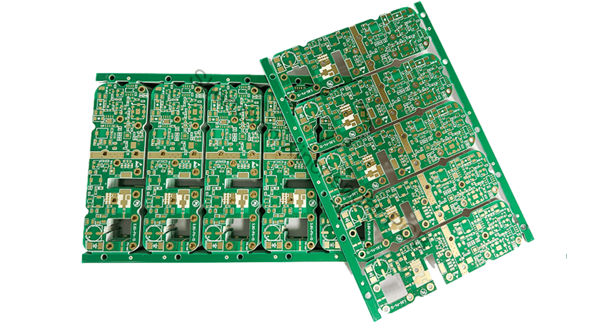
One Name, Three Machines
The confusion is not cosmetic, because it changes what a purchase order buys. A bare-board electrical tester answers one question: does the copper pattern match the netlist. It does not know what a resistor is, it does not care what will be soldered onto the board, and it runs before any component touches the panel. An in-circuit tester answers a different question: on an assembled board, does each component measure what it should, in the circuit it is actually in. A functional tester asks whether the assembly works as a system.
For a high-frequency PCB shop, the first machine is the one in scope. The second belongs to the assembly house, and the third to the product owner. Getting this wrong in a specification produces a requirement for a bed-of-nails fixture on a bare panel that has no components and no test pads sized for probes.
| Machine | Stage | Question answered | Governing reference |
|---|---|---|---|
| Bare-board electrical test | Finished bare panel | Does the netlist exist as designed — continuity and isolation | IPC-9252; acceptance per IPC-6015 / IPC-A-600G |
| In-circuit test (ICT) | After SMT and reflow | Does each component measure correctly in circuit | Customer test specification; IPC-A-610 for workmanship |
| Functional test (FCT) | After assembly, often at system level | Does the assembly perform its function | Product specification |
| RF bench test | Coupon or assembly | Impedance, insertion loss, return loss | VNA and TDR methods; coupon design per lot |
The last two rows are in the table because they are the two that high-frequency customers most often assume are covered by “electrical test” and are not. A continuity test that passes says nothing about impedance and nothing about loss. Those come from a coupon measured with a vector network analyser or a time-domain reflectometer, and the methods are set out in testing in high-frequency PCB production.
What Bare-Board Test Actually Asserts
Two assertions, both binary. Continuity: every net that should be connected is connected, measured as resistance below a threshold. Isolation: no two nets that should be separate are connected, measured as resistance above a threshold. Everything else is a refinement of those two.
The thresholds are where the engineering sits, and they are usually stated far too loosely. A continuity threshold of 10 Ω will pass a 5 Ω barrel that is nearly open, and a 2 Ω barrel is a latent failure that will open after thermal cycling. A four-wire Kelvin measurement on critical nets resolves to 0.1 Ω and is the only way to see a barrel that is thin but not yet broken. The isolation threshold is typically 10 MΩ at 100–250 V DC, and the voltage matters because a whisker or a conductive residue can pass at 10 V and break down at 250 V.
| Parameter | Typical setting | What it catches or misses |
|---|---|---|
| Continuity threshold | <10 Ω (2 Ω on critical nets) | Catches opens; misses a thin barrel at 5 Ω |
| Four-wire resistance | 0.1–10 Ω range, ±1 % | Catches a barrel that is resistive but continuous |
| Isolation resistance | >10 MΩ at 100–250 V DC | Catches shorts and leakage; voltage must be high enough to break a whisker |
| Test voltage | 50–250 V DC (higher for high-rel) | Lower voltage may pass a contaminated gap |
| Net coverage | 100 % of nets | Any net without a test point is a blind spot, not a pass |
| Test point size | ≥0.9 mm for a bed of nails; ≥0.2 mm for flying probe | Below 0.9 mm, probe pressure dents the pad |
The last row in that table drives the design conversation. A bed-of-nails fixture needs a 0.9 mm pad with 1.27 mm pitch to sit a spring probe at 100–150 g without skating off. A flying probe needs far less, down to 0.2 mm, because it addresses one point at a time and can aim precisely. That is the whole reason flying probe became the default for prototype and high-mix work: it lets the designer keep the pads small, which on a high-frequency board is not a convenience but a requirement.
Flying Probe and Universal Grid: How to Choose
The two architectures are economic answers to different questions. A universal grid tester has a fixed field of probes, typically 4,096 to 32,768, pressed onto the panel in one stroke. It is very fast per panel and very expensive per fixture. A flying probe moves two to eight heads over the panel, testing one point at a time; it is slow per panel and needs no fixture at all.
Break-even sits around a few hundred panels of the same design. Below that, fixture cost and lead time dominate and flying probe wins. Above it, the per-panel time of the flying probe becomes the constraint and the grid machine wins. High-frequency work sits almost entirely on the flying-probe side of that line, because the orders are small and the designs change.
| Attribute | Flying probe | Universal grid |
|---|---|---|
| Throughput | 5–30 points per second per head; a 2,000-net panel in 3–15 min | One stroke, 30–90 s including load |
| Fixture | None | One per design; weeks of lead time, high cost |
| Minimum pad | ≥0.2 mm | ≥0.9 mm with 1.27 mm pitch |
| Both sides | Yes, by flipping or with a dual-head machine | Yes, with a double-sided fixture |
| Four-wire | Standard on most heads | Requires dedicated probe pairs |
| Best fit | Prototype, high-mix, high-frequency, small panels | High-volume single design |
There is a third option that matters specifically on dense RF boards: capacitive coupling test. Two plates, one above and one below, form a capacitor through the copper; a moving probe on one side senses the coupling on each net, and a break in the net changes the signal. No test pads are required at all, which for a board whose lines must stay electrically clean is the decisive advantage. The limitation is equally clear — it detects opens and shorts but reports no resistance value, so it cannot find a resistive barrel.
The Test Pad Is a Discontinuity
This is the part that the standard texts on electrical test leave out, and it is the part that matters on a 28 GHz board. A test pad is a patch of copper attached to a transmission line. Electrically it is a shunt capacitance to the reference plane below, plus whatever length of stub connects it to the line.
The capacitance is easy to estimate and larger than intuition suggests. A 0.9 mm diameter pad over 0.254 mm of a 2.85 effective dielectric is about 0.06 pF. At 10 GHz that is a reactance of roughly 250 Ω in parallel with a 50 Ω line, which is a visible reflection; at 28 GHz it falls to about 90 Ω and the reflection becomes a real return-loss penalty.
| Test feature | Parasitic | Effect at 10 GHz | Effect at 28 GHz |
|---|---|---|---|
| 0.9 mm pad, in line | ~0.06 pF shunt | ~250 Ω in parallel; small reflection | ~90 Ω, measurable return loss |
| 0.9 mm pad on a 1.0 mm branch | Stub, λ/18 at 10 GHz | Notch forming above 12 GHz | Deep notch in band |
| 0.9 mm pad on a 2.0 mm branch | Stub, λ/9 at 10 GHz | Clear notch in band | Line unusable |
| 0.3 mm pad, in line | ~0.007 pF | >2 kΩ, negligible | ~700 Ω, acceptable |
| Capacitive coupling, no pad | None on the line | None | None |
Three design rules follow, and they are cheap to apply. Put the test pad in line rather than on a branch — a pad on a stub is a resonator, and its notch moves with every layer tolerance. Keep the pad as small as the chosen test method allows, which is an argument for flying probe over a fixture. And on matched lines above about 10 GHz, route the test access out to the process border and measure there, so the line inside the product outline is never touched. The impedance consequence of a badly placed pad is the same order as the whole etch tolerance; the impedance-control methodology is in impedance control and in impedance types and parameters.
The arithmetic of a full test-point population is worth doing once, because it usually settles the argument. A six-layer board with 800 nets needs 800 pads at 0.9 mm to be fully testable on a fixture. That is 800 × π × 0.45² ≈ 509 mm² of copper dedicated to testing — the area of a 22 mm square, on a board that may only be 100 mm wide. At 150 g per probe the fixture applies 120 kg to the panel in one stroke, which is why a 0.1 mm laminate needs support pins under every cluster and still deflects between them.
The practical resolution on an RF board is a split population. DC nets, supply rails, grounds and control lines get real test points, because they are where an open is both plausible and measurable at DC. Matched RF lines do not; their continuity is proven indirectly, through the net they share with a connector pin or through a coupon in the border, and their performance is proven by the coupon rather than by the tester. That split typically takes the pad count from 800 to a few hundred, removes most of the parasitic capacitance from the lines that cannot tolerate it, and leaves the fixture force low enough that a thin PTFE panel survives being probed.
What In-Circuit Test Can and Cannot See
Once the board is assembled, the bed-of-nails machine measures components in circuit: resistance, capacitance, polarity, and the presence of a device. It is fast, it is quantitative, and it is much less capable than its reputation.
It cannot see a head-in-pillow joint. That defect is a solder ball that has reflowed onto the pad but not onto the component lead, so it makes contact under probe pressure and opens when the assembly warms up in service. The probe force closes the gap the test is trying to detect, which is why a passing ICT result on a BGA is not evidence of a good joint. It also cannot see a void under a thermal pad, a crack that is still touching, or anything inside a connector body.
What it can see, and sees well: an open trace, a wrong component value, a reversed polarity, a missing part, and a short. On an RF assembly, add one more limitation — the probe itself detunes the circuit. Touching a matching network with a probe changes the impedance at that node, so an in-circuit measurement of an RF node is not the same measurement as the one the design was simulated for. This is why RF assemblies are usually tested functionally at the connector rather than node by node. The assembly-side sequence is in the PCBA manufacturing process, and the inspection-gate view in PCBA quality control.
Programming, Fixtures and the Cost of a Blind Spot
The test program comes from the CAD netlist, and the classic failure is a program that matches the CAD file rather than the fabricated board. If the CAM engineer changed a net, added a tear-drop or removed an unused pad, the program no longer describes the product, and the test will either reject good boards or, worse, pass a board with a real open because the net it was checking no longer exists.
So the program is generated from the release CAM data, and the first panel of every lot is tested and signed before the lot runs. The numbers worth tracking are escapes — nets that passed and were later found open — rather than pass rate, because a high pass rate on a badly generated program is a warning rather than a result.
Fixture cost deserves an honest line for anyone considering a grid tester. A fixture for a 2,000-point panel is a five-figure purchase with multi-week lead time, and it is specific to one design revision. On a product with a two-year life and three revisions, the fixture cost can exceed the test cost of every panel ever built. That arithmetic, not the per-panel speed, is what keeps high-frequency work on flying probe.
Acceptance Tests for the Tester
An electrical tester is a measuring instrument and has to be accepted as one. The following are the checks that separate a machine that is capable from one that merely reports.
| Test | Method | Acceptance criterion (suggested) |
|---|---|---|
| 1. Resistance accuracy | Certified resistors at 0.1, 1 and 10 Ω, four-wire | ±2 % or better; bias stated |
| 2. Repeatability | Same panel 10 times, same points | No threshold crossings; spread stated |
| 3. False opens | Known-good panel, 20 runs | <0.01 % of points — contact failure is the dominant false-call source |
| 4. Escape sensitivity | Test coupon with 2 Ω, 5 Ω and 10 Ω links | Flags at the threshold set in the specification |
| 5. Isolation voltage | Known leakage path at 100 and 250 V DC | Rejects at both, proving voltage is applied |
| 6. Probe pressure | Force gauge per head; witness marks on a test pad | 100–150 g; witness mark ≤25 % of pad area |
| 7. Pad damage | Inspect 50 probed pads under 50× | No through-plating damage; ENIG intact |
| 8. Net coverage report | Export of untested nets | Zero untested nets, or a written list accepted by the customer |
Test 7 is the one that matters most on a high-frequency build and is almost never on an acceptance list. A probe that drives through a 0.05 µm gold layer exposes the nickel beneath it, and nickel is where the current flows at 10 GHz anyway, so the surface is altered at exactly the place that carries the signal. That is acceptable on a test pad and unacceptable on a matched line, which is another argument for keeping test access in the border.
Four Claims That Do Not Survive an Audit
1. “ICT verifies signal integrity.” It measures DC resistance and component values. Insertion loss, return loss and impedance need a network analyser or a TDR, on a coupon with a known geometry.
2. “ICT detects cold solder joints.” It detects a joint whose resistance has risen enough to matter. A head-in-pillow joint measures good under probe pressure and opens at temperature, so the defect that matters most on a BGA is exactly the one the test cannot see.
3. “Electrical test is non-destructive.” Spring probes at 150 g leave a witness mark, and on a thin deposit they penetrate it. That is a controlled cost on a test pad; it is damage on a matched line, and it is why test point placement is a design decision rather than a manufacturing one.
4. “100 % electrical test means 100 % coverage.” It means 100 % of the nets that have test access. A net with no test point is not tested, and a report that does not list untested nets is not a coverage statement. The coverage report is the deliverable, not the pass stamp.
Conclusion
Two machines, two questions. The bare-board tester proves the netlist and is judged on threshold setting, four-wire capability and net coverage. The in-circuit tester proves components in circuit and is judged on what it cannot see. Neither measures impedance, and neither is a substitute for a coupon.
On a high-frequency build the design constraint is the one that is usually discovered late: testability and electrical performance pull in opposite directions, because the pad that makes a net testable is the capacitance that spoils the line. Resolving that means smaller pads, in-line placement, and test access routed into the process border — three decisions that cost nothing at the layout stage and cannot be recovered afterwards.
XCE PCB tests conventional and high-frequency builds on this basis: 2 to 72 layers, PTFE, hydrocarbon and ceramic laminates, 600×1200 mm panels, 100 % continuity and isolation to IPC-9252, four-wire resistance on critical nets, coupon impedance and loss per lot, impedance held to ±10 %, samples in as fast as 24 hours.
Frequently Asked Questions
Is ICT the same as bare-board electrical test?
What continuity threshold should be used on a high-frequency board?
Why does a test pad affect impedance?
Flying probe or bed of nails for high-frequency work?
Can electrical test find a barrel that is plated too thin?
What is capacitive coupling test used for?
Electrical Test Without Breaking Impedance?
Send us your Gerber files and requirements for a manufacturability review and a tailored quotation.
sales1@xcepcb.com
+86 180 3341 4657