
The usual explanation is that a 0.203 mm board is too thin and too fragile to survive the stress of a curing resin. That is true and it is not the reason the process fails. The process fails on three measurable constraints: at this thickness an aspect ratio near 1:1 leaves no barrel for the resin to grip, the grinding tolerance is the same size as the board thickness tolerance, and the bending stiffness is about 0.2 % of a 1.6 mm board. Each one is arithmetic, and each one has a workaround — which is why the correct answer is “not on this stack, not by this route” rather than “never”.
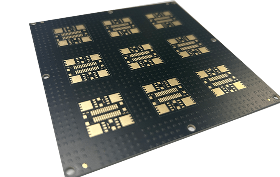
The Question Is Not About Hole Size
When a 0.203 mm stack is quoted with “resin plugged” on the via table, the refusal that comes back is usually explained as a hole-size or a fragility problem. Neither is the operative constraint. A 0.2 mm hole fills perfectly well in a 1.6 mm board, and a 0.203 mm board is not fragile in the sense of breaking in the operator’s hands. What changes at this thickness is the relationship between three numbers that are comfortable at 1.0 mm and hostile at 0.2 mm.
| Constraint | At 1.6 mm | At 0.203 mm | What it decides |
|---|---|---|---|
| Aspect ratio (thickness ÷ hole) | 6–8:1 | 1.0–1.4:1 | Whether the resin can be retained at all |
| Grinding tolerance vs thickness tolerance | ±25 µm vs ±160 µm | ±25 µm vs ±20 µm | Whether the board survives planarising |
| Bending stiffness, relative | 1.00 | 0.002 | Whether flatness can be held through the process |
The table is the whole article in three lines: at 0.203 mm the aspect ratio is too low for retention, the grinding budget is larger than the thickness budget, and the board has almost no ability to resist a local load. The sections below take each one with its arithmetic, and then set out what to do instead.
Constraint 1: An Aspect Ratio Near 1:1 Has Nothing to Grip
Filling a via is a printing and vacuum operation, and it works because the barrel provides wall area for the paste to adhere to while the vacuum pulls air out of the far end. At 6:1 there is six times the diameter in wall length, and the fill is a plug in a tube. At 1:1 the tube is one diameter long, which is closer to a hole in a sheet of paper than to a barrel.
Three things follow. The paste volume that can be retained by wall adhesion is proportional to the wall area, so a 0.2 mm hole in a 0.203 mm board holds roughly a sixth of the volume that the same hole would hold in a 1.2 mm board. The vacuum that is needed to evacuate a deep hole will, in a shallow one, pull paste straight through to the backing. And the stencil aperture has to be larger than the hole to deliver enough paste, which on a thin board means the paste column is wider than it is tall — a shape that slumps rather than stands.
The observable failure is bleed-through: resin appears on the opposite side of the panel, contaminating a surface that has already been imaged and sometimes already plated. On a 1.6 mm board this is a nuisance; on a 0.203 mm board it is a scrap event, because the opposite side cannot be cleaned without damaging the fine features that make a 0.2 mm stack worth building in the first place. The related geometry rules are in the role and key considerations for resin plugging.
Constraint 2: The Grinding Budget Is Bigger Than the Thickness Budget
After filling, the surface has to be planarised, and planarising is a grinding operation with its own tolerance. On a production line that tolerance is typically ±25 µm, and it is achieved by controlling pressure, carrier flatness and removal rate. On a 1.6 mm board that is 1.6 % of the thickness and nobody worries about it.
On a 0.203 mm board, ±10 % thickness tolerance is ±20 µm. The grinding tolerance is larger than the entire permitted variation of the part. There are then only two outcomes: the fabricator grinds to the nominal and the boards fall outside the thickness window, or he grinds to the measured thickness of each panel and the process becomes a per-panel operation with no throughput.
| Board thickness | ±10 % thickness window | Grinding tolerance | Remaining margin | Practical? |
|---|---|---|---|---|
| 0.203 mm | ±20 µm | ±25 µm | −5 µm | No — the tolerance is already exceeded |
| 0.300 mm | ±30 µm | ±25 µm | 5 µm | Only with a carrier and 100 % thickness check |
| 0.500 mm | ±50 µm | ±25 µm | 25 µm | Yes, as routine work |
| 0.800 mm | ±80 µm | ±25 µm | 55 µm | Comfortable |
The table is also the answer to the question “where is the line”. Resin plugging becomes routine at about 0.5 mm, becomes difficult at 0.3 mm and is not feasible at 0.203 mm — not because the resin changes, but because the removal tolerance stops being small relative to the part.
There is a second-order consequence that matters more than the thickness: a 0.203 mm board that is ground 5 µm too far has lost 2.5 % of its dielectric height, and on a 50 Ω line that is about 1.5 % of impedance. That sounds tolerable until it is added to the ±10 % thickness window and the etch spread — the grinding step has become an impedance variable, which it never is on a normal board.
Constraint 3: Stiffness Falls With the Cube of Thickness
Bending stiffness of a plate is proportional to the cube of its thickness, and that single relationship explains most of what goes wrong. A 0.203 mm board is 12.7 % of the thickness of a 1.6 mm board, so it has 0.205 % of its stiffness — two parts in a thousand.
| Thickness | Relative stiffness (1.6 mm = 1) | What it can tolerate |
|---|---|---|
| 0.203 mm | 0.002 | Nothing local — grinding pressure, conveyor rollers and a tape pull all deform it |
| 0.300 mm | 0.007 | Carrier required through grinding |
| 0.500 mm | 0.031 | Handles normal handling; still warps if the stack is asymmetric |
| 0.800 mm | 0.125 | Normal process, normal care |
| 1.600 mm | 1.000 | Reference |
Stiffness matters here because planarising is a pressure operation, and the pressure has to be resisted by something. On a 1.6 mm board the panel resists and the resin at the via is the only thing that yields. On a 0.203 mm board the panel itself yields, so the grinder removes material from the high spots of a deforming sheet — and the result is a board that is flat while it is held and warped when it is released. That is the mechanism behind the complaint that a thin board “looks fine and then will not sit flat in the assembly fixture”.
The same property shows up in handling. A 0.203 mm panel cannot be conveyed on rollers without support, cannot be baked flat without a weight or a carrier, and cannot be probed without a vacuum bed. Every one of those is a normal requirement of thin-board processing and none of them is compatible with a grinding step that needs uniform contact pressure.
The Plating Specification Decides More Than the Resin Does
Once the resin route is set aside, the reliability of a thin PTFE board rests on the barrel, and the numbers there are specific. Barrel copper of 20–25 µm with elongation of at least 20 % is what absorbs the 4 % differential strain described above; a deposit that meets the thickness and misses the elongation is a barrel that measures well on a section and cracks at the customer’s reflow.
Thin boards invert one of the usual plating problems. On a 6:1 hole the difficulty is throwing copper to the middle; on a 1:1 hole the throw is trivial and the problem becomes the surface. With the barrel plating easily, the surface copper climbs past 42 µm, and on a 0.203 mm stack the outer-layer line width is already narrow because the dielectric is thin — a 50 Ω microstrip on 0.203 mm of Dk 3.38 is about 0.45 mm, so 10 µm of extra plating on each side is a 4 % width change and roughly 2 % of impedance.
What this means in practice is that the plating thickness on a thin board has to be specified as a window rather than a minimum, and the etch compensation has to be released against the plated thickness rather than the base foil. That is an unusual instruction for a fabrication drawing and it is the right one here.
The Thermal Account at 0.203 mm
The stress argument in the usual explanation is correct but it is usually left unquantified, and the numbers are smaller than people expect — which is why the stress alone is not the reason to refuse the process. Over a reflow excursion of 215 °C, a 0.203 mm PTFE board expands about 10 µm in Z while a cured plug expands about 2 µm.
| Material | Z CTE (ppm/°C) | Expansion over 0.203 mm at ΔT = 215 °C |
|---|---|---|
| RT/duroid 5880 | 237 | 10.3 µm |
| TLY-5 | 217 | 9.5 µm |
| RO4003C | 46 | 2.0 µm |
| RO4350B | 32 | 1.4 µm |
| Plugging resin | 40–60 | 1.7–2.6 µm |
| Copper barrel | 17 | 0.7 µm |
An 8 µm differential over a 0.203 mm length is a strain of about 4 % — not trivial, and within the capacity of a barrel plated with copper at 20 % elongation, which is exactly why the plating specification matters more than the resin on a thin PTFE board. What the strain does to a thin board is different from what it does to a thick one: on a thick board the laminate constrains the movement and the barrel absorbs it; on a 0.203 mm board the constraint is absent, so the same strain shows up as local warpage and as separation at the resin-to-wall interface, where there is only 0.2 mm of bond line to resist it.
This is the honest version of the “board burst” failure: it is not that the stress is larger at 0.203 mm — it is the same stress per unit of CTE — but that the structure that distributes it has gone. The plating and via rules behind that statement are in PCB through holes and plating high-frequency PCB.
What Actually Happens in the Oven
If a 0.203 mm board is plugged and planarised anyway, the failures appear in a predictable order, and knowing the order is useful because it tells you which one you will see first.
First, bleed-through. Resin appears on the reverse side during the fill, before curing, and the panel is contaminated. This is the failure that stops the process at 1:1 aspect ratio irrespective of everything else, because it happens before the board has a chance to warp.
Second, depression at the via. Because the paste column is wider than it is deep, cure shrinkage shows as a dish rather than as a shrink along the barrel. A 0.203 mm fill with 0.3 % linear shrinkage loses about 0.6 µm of depth — small in absolute terms, but the target is ≤25 µm and the planarising tolerance is already eating the budget.
Third, warpage after bake. The plug occupies a different volume fraction of the board than at 1.6 mm — the same via diameter in a much thinner board — so the resin volume is a larger share of the cross-section and its cure shrinkage is a larger share of the internal stress. On a board with 0.2 % of normal stiffness, that stress warps the panel.
Fourth, cap cracking. If the via is capped, the cap is 20–25 µm of plated copper over a resin column with a different CTE. At a 4 % differential strain over 0.203 mm the cap is the least compliant element in the stack, and a crack there is invisible until the assembly fails an electrical test.
The 0.3 mm Middle Case: What Changes and What Does Not
Between the impossible and the routine sits a thickness that is often the one a design actually needs. At 0.3 mm the stiffness is 0.7 % of a 1.6 mm board — three times the 0.203 mm value, which is still almost nothing in bending but enough that a carrier can hold the panel flat through grinding.
The arithmetic moves in a way that is easy to follow. The thickness window becomes ±30 µm against a grinding tolerance of ±25 µm, which leaves 5 µm of margin: not comfortable, but not negative. The aspect ratio for a 0.2 mm hole becomes 1.5:1, which still bleeds through on a plain fill, so the back side needs a dry film or a sacrificial copper layer to act as a stop. And the resin volume as a share of the cross-section is still high enough that warpage after cure has to be controlled by a symmetric stack rather than by the board’s own stiffness.
So 0.3 mm is feasible rather than routine: it works with a carrier, a back-side stop and a hundred per cent thickness check, and it costs perhaps 1.5–2× a normal plugging operation. That is a different answer from 0.203 mm, and it is worth knowing because a 0.1 mm increase in stack height is often available in the mechanical envelope when the designer is told what it buys.
Five Ways Out, Ranked
None of this means a 0.203 mm stack with vias in pads is impossible. It means the resin route is the wrong route, and there are five alternatives that work, in order of how little they change.
| Option | What changes | Feasibility at 0.203 mm | Cost and risk |
|---|---|---|---|
| Solder-mask plug (IPC-4761 Type II or III) | No grinding; the via stays slightly dished | Routine | Cheapest; no flat pad, so no via-in-pad |
| Escape the via out of the pad | Layout: a short stub trace to a via beside the land | Routine | Uses routing space; needs a design change |
| Copper-filled via (plating) | No resin; no CTE mismatch, no grinding of a dielectric | Possible at this aspect ratio | Needs a bath with a good via-fill additive; still planarised |
| Thicken the stack to 0.4–0.5 mm | The product envelope | Becomes routine work | Changes the mechanical design; 0.5 mm has 15× the stiffness |
| Carrier plus single-sided grind | Process only: bonded to a carrier for grinding | Marginal at 0.203 mm | Expensive; low throughput; needs 100 % thickness check |
The third option deserves a note because it is often overlooked. Copper-filled vias are electroplated, so there is no resin to shrink and no dielectric plug with a different CTE — the fill is the same metal as the barrel. What they need instead is a plating chemistry with a via-filling additive and an aspect ratio the chemistry can handle, which in practice is under about 0.8:1 for a full bottom-up fill. A 0.1 mm hole in a 0.203 mm board is 2:1 and will not fill bottom-up; a 0.25 mm hole at 0.8:1 will. So the option exists and it is constrained by the same geometry, just in the opposite direction.
The HDI context for this trade is in the HDI production process, and the impedance consequence of thinning the dielectric is in common impedance designs and layer stacks.
Cost: What Each Route Actually Saves
The five options differ in where the money goes rather than in whether money is spent. A carrier-based plug on a 0.203 mm board is expensive because the carrier, the single-sided grind and the hundred per cent thickness check are all per-panel operations, and the throughput loss is larger than the material cost. An escape route costs routing space and a design revision, which is free at layout and expensive after tooling.
| Route | Where the cost lands | Yield risk | When it is the right answer |
|---|---|---|---|
| Type II or III mask plug | Nothing extra — it is in the standard flow | Low | The via is not under a land |
| Escape the via | Layout area and a revision | Low | Inner layers have room; no flatness requirement |
| Copper-filled via | Plating capability; a bath with a filling additive | Medium — plating-dependent | The pad must be flat and the hole is at 0.8:1 or better |
| Thicken to 0.4–0.5 mm | Mechanical envelope only | Lowest | The product has 0.2–0.3 mm to spare |
| Carrier plus single-side grind | Per-panel operations, throughput | Highest | Nothing else fits — accept the cost |
Ordered by cost, the list is almost the reverse of the list ordered by how much the design is willing to change, which is why these conversations stall. The cheapest route requires a layout change and the most expensive route requires none, so a team that starts from “the drawing is frozen” has already chosen the worst option without noticing. Raising the question at the stack review, before the netlist is locked, is worth more than any negotiation at the quotation stage.
What to Put on the Drawing Instead of “Resin Plugged”
The most useful outcome of this analysis is a specification that a fabricator can quote against without inventing an interpretation. Four items cover it.
Name the IPC-4761 type for each via class rather than writing “plugged”, because Type II, Type V and Type VII differ by more than a factor of three in cost and by the presence or absence of a grinding step.
State whether the via is in a land, and at what pitch. A 0.4 mm pitch land over a via requires a flat cap, which on a 0.203 mm board is the item that most often forces a redesign.
Give the thickness window you actually need, not the nominal. If the assembly tolerates 0.203 mm ±15 % rather than ±10 %, the grinding budget alone becomes feasible and the question changes from “can this be done” to “what does it cost”.
Allow the alternative explicitly. A drawing note permitting a solder-mask plug on non-critical vias, or an escape route on a via that does not have to be in the pad, removes the most common reason a 0.203 mm quote comes back either very expensive or declined. The stack side of the same conversation is in lamination in high-frequency PCB manufacturing and drilling high-frequency PCB.
Conclusion
Resin plugging is not feasible on a 0.203 mm high-frequency board for three reasons, and only the third is about strength. At an aspect ratio near 1:1 there is no barrel to retain the resin, so a vacuum fill pushes paste through to the other side. The planarising tolerance of ±25 µm is larger than the entire ±20 µm thickness window, so the board cannot survive the step that makes the plug useful. And with 0.2 % of the stiffness of a 1.6 mm board, the panel cannot hold flatness through a pressure operation, so the result is flat in the fixture and warped in the assembly.
The thermal mismatch adds to it rather than causing it: about 10 µm of Z expansion against 2 µm of plug movement over a reflow excursion is a 4 % strain, which a properly plated barrel absorbs and a thin board cannot distribute.
The way forward is neither to insist nor to abandon. Move the via out of the pad, or use a solder-mask plug where flatness is not required, or thicken the stack to 0.4–0.5 mm where the same fill becomes routine, or use a copper-filled via if the plating chemistry suits the geometry. XCE PCB quotes these alternatives against the actual stack rather than against a category, on 2 to 72 layers with PTFE, hydrocarbon and ceramic laminates, 600×1200 mm panels, impedance ±10 %, samples in as fast as 24 hours, inspected to IPC-A-600G and IPC-6015.
Frequently Asked Questions
At what board thickness does resin plugging become practical?
Why does resin bleed through to the other side of a 0.203 mm board?
Is the problem that a 0.203 mm board is too weak to take the resin stress?
Can a copper-filled via replace a resin plug on a thin board?
What should a drawing say instead of “resin plugged”?
Does a 0.203 mm stack with vias in pads have to be redesigned?
Have a 0.2 mm Stack That Needs Flat Vias?
Send us your Gerber files and requirements for a manufacturability review and a tailored quotation.
sales1@xcepcb.com
+86 180 3341 4657