
HDI PCB is usually introduced by its benefits — denser, faster, smaller — and by a layer count, which is the one thing that does not define it. A six-layer board with 0.3 mm through holes is not HDI; a four-layer board with 0.1 mm laser vias is. The definition is a single geometric inequality: a microvia is a hole of 150 µm or less whose aspect ratio is at most 1:1, which means the dielectric it passes through can never be thicker than the hole is wide. Every structural feature of HDI — the build-up sequence, the way vias are stacked, the capture land, the density limits and the cost multipliers — is a consequence of that one constraint.
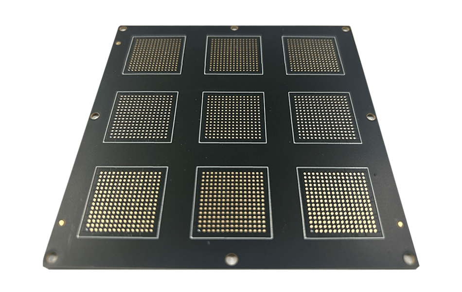
The Definition Is an Inequality, Not a Layer Count
A high-density interconnect board is a board whose connections between layers are made with microvias, and a microvia is defined geometrically: a hole of 150 µm or less, formed by laser or by photo-definition, with an aspect ratio of at most 1:1 and preferably 0.75:1. Aspect ratio here is depth over diameter — the thickness of dielectric the hole passes through, divided by the hole diameter.
The consequence is not a matter of degree. If a 100 µm hole may only be 100 µm deep, and preferably 75 µm, then every dielectric layer that a microvia crosses must be 75–100 µm thick. That is why HDI is built by lamination of thin films onto a finished core, rather than by drilling through a conventional stack: the constraint is on the dielectric, and only a build-up process can make dielectric that thin one layer at a time.
| Via diameter | Depth allowed at 1:1 | Depth at the preferred 0.75:1 | Formation method | Typical use |
|---|---|---|---|---|
| 150 µm | 150 µm | 112 µm | CO₂ laser, single pulse | First build-up layer on heavy panels |
| 100 µm | 100 µm | 75 µm | CO₂ laser, optimised | The mainstream HDI via |
| 75 µm | 75 µm | 56 µm | UV laser or conformal-mask CO₂ | Fine-pitch mobile and module boards |
| 50 µm | 50 µm | 38 µm | UV laser, thin film only | Advanced packaging substrates |
| 0.30 mm mechanical | — | — | Mechanical drill | Not a microvia, whatever the layer count |
The last row is the one that settles most arguments about whether a board is HDI. A mechanically drilled through hole, at any diameter, is not a microvia; a board whose only interlayer connections are mechanical holes is a conventional multilayer board, even if it has twenty layers and 75 µm lines. Density alone does not make HDI — the via structure does.
The Case That Looks Like HDI and Is Not
The clearest counter-example is a thin PTFE board. Take a 0.254 mm high-frequency laminate, where the whole dielectric is 254 µm. A through via at an aspect ratio of 1:1 would have to be 254 µm across, which is larger than the 150 µm definition allows. To bring it inside the microvia definition the hole must come down to 150 µm or less, and then the dielectric must come down with it — which, on a single 0.254 mm core, it cannot, because the core is the dielectric.
So a thin PTFE radio board is dense, is often drilled with small holes and is frequently described as HDI, and is not: it is a conventional board whose holes are small because the board is thin. The distinction matters commercially, because microvia capability is what buyers audit and because the process qualification is different — laser drilling of PTFE requires different absorption behaviour, and the desmear chemistry is sodium-naphthalene or plasma rather than permanganate.
A second case is the board with a single blind via layer added for convenience. That is HDI in structure if the vias are microvias, but it is a 1+N+1 build with no stacking, and its density ceiling is set by the core, not by the build-up. The next two sections are about saying which of these a design actually needs.
Type I, II and III: The Three Structures
The standard classification follows IPC-2226 and describes how many build-up layers are added on each side of a core. What it encodes is the number of lamination cycles, because that is what the customer pays for and what the registration error accumulates across.
| Type | Structure | Typical layer count | Via content | Where it is used |
|---|---|---|---|---|
| Type I | One build-up layer each side, no stacked microvia | 6 layers (1+4+1) | Microvias to the core, plus through holes | Modules, industrial control, first-generation mobile |
| Type II | One build-up each side, with at least one stacked microvia | 6–8 layers | Microvia on microvia at least once | Smartphones, wearables, camera modules |
| Type III | Two or more build-up layers each side, core carrying through holes | 8–12 layers (2+4+2 and up) | Stacked or staggered microvias, buried vias in the core | High-end handsets, SiP substrates, advanced automotive |
| ELIC | Every layer interconnected, no core through hole | 8–16 layers | Copper-filled stacked vias layer on layer | Flagship processors, high-layer-count substrates |
Two things are worth noting about this table. The layer counts are indicative rather than definitional — an 8-layer Type I and an 8-layer Type III are both possible, and differ in where the through holes are. And ELIC is a different proposition rather than a bigger Type III: with no through hole there is no core, so every layer is a build-up layer, the panel goes through the press eight or more times, and the yield arithmetic in the next section changes sign.
Stacked, Staggered, Skipped: The Via Schemes and Their Cost
Once a design needs two build-up layers on a side, there is a choice about how the two microvia layers connect. A staggered scheme offsets the upper via from the lower one and connects them through a copper landing pad; a stacked scheme puts them on the same axis and connects them directly, metal to metal; a skipped scheme passes a via over an intermediate layer to reach a deeper one.
| Scheme | How it is built | Registration demand | Yield experience | Cost multiplier |
|---|---|---|---|---|
| Staggered | Upper microvia lands on a pad over the lower one | Loosest; each layer aligned to its own target | 96–98 % on the via chain | 2+N+2 baseline |
| Stacked | Upper microvia directly on the lower, filled and capped | Tight; the alignment of both cycles applies to one column | 91–94 % | +15–25 % over staggered |
| Skipped | Via passes over one layer to reach a deeper target | Deep drill through two dielectrics at once | 89–92 % | +10–20 % |
| ELIC | All layers stacked, no core | Cumulative over every cycle | Lowest per panel; recovered by density | 2–3× |
The yield column is not a law of physics but it is a law of error accumulation, and the arithmetic is simple. Registration error per lamination cycle is roughly ±25 µm and, for a stacked column, the errors of all cycles apply to the same axis. A 100 µm via inside a 250 µm capture land leaves 75 µm of land on each side at nominal; two cycles of ±25 µm consume two thirds of that margin, and three consume all of it. That is why the practical answer, when a design can be routed either way, is to stagger — the density gain from stacking is smaller than the yield loss, unless the pitch leaves no landing pad at all.
The process controls behind those numbers, station by station, are set out in HDI PCB manufacturing process; the electrical consequences of the same structures are in HDI PCB performance. This article stays with the structural decision.
Capture Land: The Geometry That Sets the Density Ceiling
A microvia needs a pad, and the pad is larger than the hole by twice the annular ring. For a 100 µm laser via the land is typically 250 µm, giving 75 µm of ring on each side — not because 75 µm is needed for current, but because registration and laser-drill position error consume it.
| Microvia | Capture land | Ring per side | Error budget at ±25 µm/cycle | Consequence at two cycles |
|---|---|---|---|---|
| 75 µm | 200 µm | 62 µm | 50 µm used | 12 µm left — stacked schemes at this size are marginal |
| 100 µm | 250 µm | 75 µm | 50 µm used | 25 µm left — workable, no room for a third cycle |
| 150 µm | 350 µm | 100 µm | 50 µm used | 50 µm left — the reason first build-up layers use bigger vias |
This is the quiet reason HDI density saturates. Halving the via diameter does not halve the pad: the ring is set by process error, not by geometry, so shrinking from 150 to 100 µm saves 100 µm of pad and shrinking from 100 to 75 µm saves only 50 µm, while the yield cost rises. Below about 75 µm the pad is dominated by the error term and the economics stop working for anything except substrate-like processes.
What Pitch Forces: The Build-Up Decision in One Table
The decision between a conventional board, 1+N+1, 2+N+2 and ELIC is forced by the pitch at the package edge, because the number of traces that must leave a row of pads per unit of width is fixed by geometry. One trace needs a width and two clearances; a via between pads needs a pad and two clearances; two traces need two widths and three clearances.
| BGA pitch / channel width | Traces per channel | What it requires | Structure |
|---|---|---|---|
| 1.0 mm / 0.5 mm | 2 at 0.1 mm line, 0.1 mm gap | Nothing special; through-hole fan-out works | Conventional multilayer |
| 0.8 mm / 0.35 mm | 1 trace beside one via | 0.3 mm via, 0.15 mm line | Conventional, 0.15 mm class |
| 0.65 mm / 0.30 mm | Exactly 1 at 0.1 mm | 0.25 mm via, or microvia | 1+N+1 boundary |
| 0.50 mm / 0.20 mm | 1 at 0.075 mm line, 0.06 mm gap | Via-in-pad or laser via between pads | 2+N+2 |
| 0.40 mm / 0.15 mm | 1, and no room for a via between pads | Via-in-pad with filled and capped microvia | 2+N+2 or 3+N+3 |
The 0.65 mm row is the one to remember: below it, a conventional through via cannot fit between pads at any line width, and the board has crossed into HDI whether or not anyone calls it that. Above it, HDI buys density and signal integrity but is not required, which is why the decision should be made from the package footprint rather than from a product category.
Dielectric Thickness: The Constraint Nobody Escapes
Because a 100 µm microvia may only cross 75–100 µm of dielectric, the build-up film is specified in that range, typically 60–80 µm after cure and ±10 % on thickness. That number reaches the electrical design directly, because the impedance of a trace on the build-up layer is set by its width relative to 60–80 µm.
On a build-up dielectric of Dk 3.4, a 50 Ω microstrip on 75 µm of film is about 0.17 mm wide — wide, not fine. Which is worth stating plainly, because it inverts an assumption: the fine-line capability of HDI is not what limits RF routing. On a 75 µm dielectric, 50 Ω is a comfortable width, and the real limitation is the loss of the material: build-up films have a dissipation factor of 0.015–0.025, which is four to eight times worse than a hydrocarbon RF laminate and twenty times worse than PTFE.
That is the whole basis of the split that appears in every HDI radio module: the RF traces and the antenna feed stay on the core, using a low-loss laminate, and the build-up layers carry digital and power. The material side of that argument is quantified in materials and their properties for HDI PCB; the impedance arithmetic is in impedance control in high-frequency PCB manufacturing.
Density: Three Numbers Instead of the Word “High”
Density is measurable, and three quantities cover most of it: the finest line and space, the number of interlayer connections per unit area, and the pad-to-pad pitch that all of it has to fit between. Stating all three is what separates a real capability from an adjective.
| Metric | Conventional board | 1+N+1 | 2+N+2 | What sets the limit |
|---|---|---|---|---|
| Minimum line / space | 0.10 / 0.10 mm | 0.075 / 0.075 mm | 0.050 / 0.050 mm | Etch and plating on thin copper, not lithography |
| Microvia diameter | — | 100 µm | 75 µm | Laser spot and dielectric thickness |
| Interlayer connections per cm² | 40–80 | 150–300 | 400–800 | Capture land and pitch |
| Smallest escape pitch | 0.8 mm | 0.65 mm | 0.4 mm | Traces per channel, as in the previous table |
These are capability classes, not guarantees, and the honest form of a supplier claim names the class and the acceptance criteria together — for example 75 µm microvia at 1:1 with a filled and capped finish, inspected to IPC-6016, with a stated coupon for the via chain.
Where the Cost Comes From
HDI is expensive for four reasons, and only one of them is the laser. The others are the number of press cycles, the yield of the via chain, and the panel utilisation loss from thin build-up films.
| Cost driver | What it adds | Why |
|---|---|---|
| Each lamination cycle | One press, one registration (±25 µm), one inspection | 1+N+1 has two; 2+N+2 has four; ELIC has one per layer |
| Laser drilling | 0.3–0.6 s per via plus tooling per panel | Throughput, not consumables, dominates |
| Via fill and planarisation | Paste fill, cure, grinding, plating over | Required for via-in-pad; voids under 2 %, dimple under 25 µm |
| Yield | Compounding per cycle | 98 % per cycle at four cycles is 92 % overall, before electrical test |
The multipliers that follow are consistent across suppliers: 1+N+1 adds 30–40 % to a conventional board of the same layer count, 2+N+2 adds 60–100 %, and ELIC is two to three times the conventional price. That ladder, not the via count, is the number to put in front of a programme manager when the package footprint is still negotiable.
When HDI Is the Wrong Answer
Four situations in which a microvia structure costs money and returns nothing. First, when the pitch is 0.8 mm or coarser and the routing fits — a conventional board at 0.1 mm lines will escape it. Second, when the constraint is thermal rather than electrical: a microvia of 100 µm plated at 25 µm wall carries very little heat, and a filled 0.25 mm through via is a better thermal path than a stack of small ones. Third, when the board is thick high-frequency laminate with a single dielectric layer, as described earlier — there is nothing to build up onto.
Fourth, and most often overlooked, when the product volume is low. The tooling and set-up of a build-up process is per design and per layer count, so a 1+N+1 board at a hundred pieces costs more per unit than a conventional board with a larger package and an extra pair of layers. HDI is a density purchase, and density is only worth buying when the alternative is a larger product or a longer route.
Two Stack-Ups, Written Out
Concrete stacks make the structure legible. The first is a 6-layer Type I with one build-up layer per side and a 0.8 mm core pair; the second is an 8-layer Type III with two build-up layers per side, used when the pitch falls below 0.5 mm.
| 6-layer 1+4+1 | 8-layer 2+4+2 | |
|---|---|---|
| L1 | Signal, 100 µm microvia to L3 | Signal, 75 µm microvia to L2 |
| L2 | Ground plane (core) | Ground, 100 µm microvia to L3 (staggered) |
| L3 | Signal / power (core), through vias | Signal (core), buried vias |
| L4–L5 | Ground and power (core) | Core power and ground |
| L6 | Signal, microvia to L4 | Signal, microvia to L7 |
| L7–L8 | — | Ground (core), signal with 75 µm microvias |
| Press cycles | 2 | 4 |
Note what is absent from both: a microvia that does not land on a plane or a pad. Every one of them terminates on copper at both ends, which is the same rule the thermal path needs — a filled via that ends on a signal layer is a dead end for heat as well as for current, as described in thermal management in PCB manufacturing.
Specification Checklist for an HDI Enquiry
Seven items turn an HDI enquiry into a quotation that can be compared. The via structure by layer pair: diameter, laser or mechanical, filled or plated, and whether it is stacked or staggered. The build-up type: 1+N+1, 2+N+2, 3+N+3 or ELIC. The dielectric thickness per build-up layer, with tolerance. The core material and thickness, separately from the build-up. The capture land and the resulting annular ring. The finish over filled vias, with the dimple limit. And the acceptance document: IPC-6016 for the build-up, IPC-6012 class 3 for the core, plus the via-chain coupon that will be measured.
XCE PCB builds 1+N+1 and 2+N+2 HDI on FR-4, hydrocarbon and PTFE cores from 2 to 72 layers total, with 100 µm laser vias, filled and capped via-in-pad, impedance held to ±10 %, panels to 600×1200 mm and samples in as fast as 24 hours. The stack, including the core, is designed together with the build-up because the two cannot be optimised separately — see high-frequency PCB stack-up design — and where a microvia has to be laser-drilled into PTFE, the preparation route is in lamination in high-frequency PCB.
Conclusion
HDI is defined by one inequality: a microvia is 150 µm or less, its aspect ratio is 1:1 or less, and therefore the dielectric it crosses is at most as thick as the hole is wide. Everything in this article follows from it. The build-up process exists because thin dielectric cannot be made any other way. The Type I–III classification counts press cycles, because that is where the error accumulates. Stacked vias cost more and yield less than staggered ones for the same reason. The capture land stops shrinking below about 75 µm because the ring is set by registration error rather than by geometry. And the electrical limit on a build-up layer is not line width — 50 Ω on 75 µm of film is 0.17 mm — but the dissipation factor of the film, 0.015–0.025.
The practical version: decide HDI from the package pitch, choose the number of build-up layers from the traces per channel, stagger wherever the land allows, and keep the radio on the core. Those four sentences cover the structural decision, and they are all arithmetic.
Frequently Asked Questions
What actually makes a PCB an HDI board?
Is a thin 0.254 mm PTFE board HDI?
Should vias be stacked or staggered?
What is the smallest BGA pitch that still avoids HDI?
Why is a 50 ohm line on an HDI build-up layer not especially narrow?
How much does HDI add to the price?
Have a Pitch That Only HDI Can Escape?
Send us your Gerber files and requirements for a manufacturability review and a tailored quotation.
sales1@xcepcb.com
+86 180 3818 8537