
Every high-frequency PCB supplier lists the same advantages — experience, advanced equipment, strict quality control, material expertise, engineering support. The list is worthless not because the claims are false but because none of them can be checked. This article takes the advantages of Shenzhen Xinchenger Electronics and rewrites each one as a number with a document behind it: 2–72 layers, panels to 600×1200 mm, impedance ±10 %, samples in 24 hours for defined builds, 10,000 m² a month from a 5,000 m² plant, 80+ engineers, production since 2009. Each section also says what the number does not cover, because that is the part a purchasing engineer actually needs.
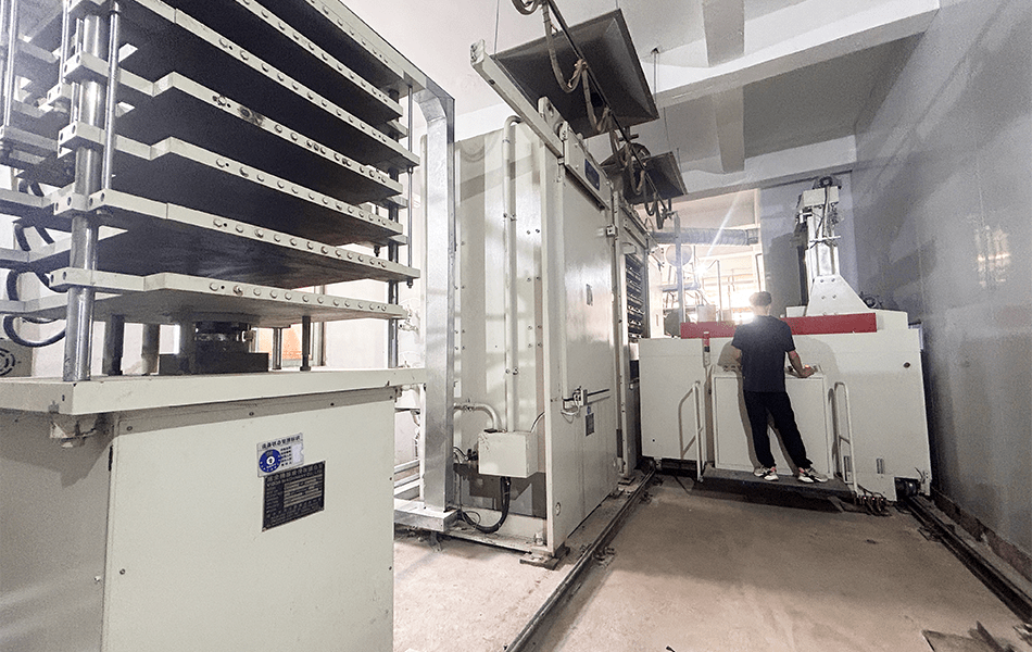
A Claim Becomes an Advantage Only When It Can Be Checked
The original version of this page listed seven strengths in about 860 words and contained no number at all. “Extensive experience”, “advanced production equipment”, “strict quality control” — each phrase is true of every fabricator in Shenzhen, which means each phrase distinguishes none of them. A purchasing engineer reading it cannot form a question, and a question is the only thing that turns marketing into a decision.
So the seven sections below are built the other way round. Each starts from a number we are willing to be held to, then names the document or measurement that proves it, then states the boundary — the case the number does not cover. That third part is what makes the first two credible: a supplier who never states a limit has either not measured it or is not telling you.
| Claim | The number we publish | What you can ask for |
|---|---|---|
| Experience | Manufacturing since 2009; more than 10,000 builds shipped | A traveller from a comparable build: material lot, stack, press cycle, test data |
| Layer range | 2 to 72 layers | Stack-up drawing plus a cross-section from a build above 20 layers |
| Panel size | Up to 600×1200 mm | Panel utilisation sheet for your array, with the grain direction marked |
| Impedance | ±10 % on controlled-impedance layers | Coupon report: layer, coupon geometry, instrument, frequency, temperature |
| Prototype | Samples in as fast as 24 hours on defined builds | The exclusion list — what 24 hours does not include (see section 8) |
| Output | 10,000 m² per month from a 5,000 m² plant | Booked versus free capacity for the month you need |
| Engineering | 80+ engineers, including CAM and stack-up review | The name of the engineer who signs your stack-up, and their response time |
| Acceptance | Inspected to IPC-A-600G and IPC-6015 | The class written on the drawing, and the AQL applied to each defect type |
Eight rows, eight numbers, eight documents. Everything else in this article is the explanation of why those particular numbers were chosen and where they stop.
Experience Is a Yield Number, Not a Duration
Seventeen years of production is easy to state and hard to interpret. What accumulates in a high-frequency shop is not general knowledge; it is a set of recipes for specific material-and-geometry combinations, and the recipes only matter where the material behaves badly.
Take the coefficient of thermal expansion through the thickness, which is the number that decides whether a plated hole survives assembly. On a 1.6 mm board taken through one 215 °C reflow, a PTFE laminate with microglass expands about 4.4 % in Z and moves roughly 82 µm; Taconic TLY-5 is close behind at 4.0 % and 75 µm. A hydrocarbon thermoset such as RO4350B moves 0.30 %, which is 11 µm. A conventional FR-4 in the glassy state sits at 17–24 µm.
| Laminate | Z expansion, one reflow | What it forces in the process |
|---|---|---|
| RT/duroid 5880 | about +82 µm (4.4 %) | Plating with ≥20 % elongation; aspect ratio held to 6:1; reflow count treated as a finite resource |
| Taconic TLY-5 | about +75 µm (4.0 %) | Same plating class; sodium-naphthalene or plasma desmear, never permanganate |
| RO4350B | about +11 µm (0.30 %) | Standard IPC Class 2 plating is adequate; the risk moves to lamination voids instead |
| FR-4 (below Tg) | 17–24 µm | Ordinary process; the constraint is drill wear, not Z expansion |
The number is the easy part; the recipe is the advantage. A shop that has only run 5880 a few times will drill it at an aspect ratio it survives on FR-4 — 8:1 or 10:1 — and the boards will pass electrical test and fail in the second reflow, months later, with the failure attributed to the customer’s assembly. Seventeen years buys the knowledge that 6:1 is the ceiling on PTFE, that desmear chemistry is not interchangeable between families, and that a 0.25 mm finished hole in 1.6 mm of PTFE is above that ceiling before anyone starts.
The visible consequence is first-pass yield on the difficult builds, which is the number to ask about rather than the year the company was founded. The process sequence those recipes belong to is set out in the twelve steps of high-frequency PCB manufacturing.
Equipment Is a Set of Windows, Not a List of Machines
A machine list answers the wrong question. What determines whether a board can be built is the window each machine holds — the temperature, pressure, tolerance and time inside which the material behaves — and whether those windows can be visited in a sequence that the laminate survives.
Nothing illustrates this better than lamination, because the three material families used in high-frequency work cure in three disjoint windows.
| System | Press window | Bonding layer | Consequence |
|---|---|---|---|
| FR-4 | 170–190 °C | FR-4 prepreg, Tg-matched | Standard cycle; can be sequenced with RO4000 in a second press |
| RO4000 series | 190–200 °C | RO4450 bondply or 4000-series prepreg | Needs its own cycle; PTFE cannot be in the same book |
| PTFE + FEP | 260–300 °C | FEP film or 3001 bondply at 290–315 °C | Far above FR-4 degradation in oxygen; separate press, separate tooling |
The practical reading is that a hybrid board is not one lamination, it is two or three, and the order matters: the PTFE sub-assembly is usually pressed first because it is the one that cannot be re-pressed, then bonded to the FR-4 core at the lower window. That is why a four-layer hybrid with one PTFE layer costs more than a six-layer all-FR-4 board of the same size, and why a quote that ignores the sequencing is a quote that will be revised after the first build.
Two more windows decide yield before a single hole is drilled. In cutting, a 600 mm panel of TLY-5 grows about 0.31 mm over a 20 °C rise, so the panel is rough-cut with 3–5 mm of margin, allowed to relax, then finish-cut — and PTFE is never laser-cut, because above 400 °C it decomposes and releases hydrogen fluoride. In drilling, the finished hole is the drill diameter minus twice the plating thickness, so 25 µm of copper per wall turns a 0.30 mm drill into a 0.25 mm hole; in 1.6 mm of PTFE that is an aspect ratio of 6.4:1 and outside the window, which is why the drill is opened to 0.35 mm or the board is thinned. The cutting side of the same problem is covered in substrate cutting for high-frequency PCBs.
Material Expertise Is Measured in Parameters, Not Brand Names
“Experienced with Rogers, Taconic and PTFE” is the most repeated sentence in this industry and the least informative. The materials differ along five axes that no single number captures, and a shop that cannot quote them from the data sheet is not selecting material, it is reading a catalogue.
| Laminate | Dk (process) | Df | TCDk (ppm/°C) | CTE x/y/z (ppm) | Peel / conductivity |
|---|---|---|---|---|---|
| RO3003 | 3.00 ±0.04 | 0.0010 | — | 17 / 16 / 25 | 0.50 W/m·K |
| RO4350B | 3.48 ±0.05 | 0.0037 | +50 | 10 / 12 / 32 | 0.88 pli / 0.69 W/m·K |
| RT/duroid 5880 | 2.20 ±0.02 | 0.0009 | −125 | 31 / 48 / 237 | 5.5 N/mm / 0.20 W/m·K |
| Taconic TLY-5 | 2.20 ±0.02 | 0.0009 | — | 26 / 15 / 217 | 3.04 N/mm |
| RO6010.2LM | 10.20 ±0.25 | 0.0023 | −425 | 24 / 24 / 47 | 12.3 pli / 0.86 W/m·K |
| RO6035HTC | 3.50 ±0.05 | 0.0013 | −66 | 19 / 19 / 39 | 7.9 pli / 1.44 W/m·K |
Three errors follow from treating the family as interchangeable, and all three are common enough that a buyer should test for them in conversation. First, PTFE and hydrocarbon are not the same polymer: RT/duroid 5880 is PTFE with micro-glass, RO4350B and RO4003C are hydrocarbon/ceramic thermosets, and the process consequences — sodium-naphthalene desmear, 6:1 aspect ratio, cold flow under pressure — apply to the first and not the second. Second, one model’s parameters do not transfer across a series: RO3003 is 3.00 and 0.0010 while RO3010 in the same family is 10.2 and 0.0022, and RO3010 also has a design Dk of 11.20 that differs from its process Dk — quoting the wrong one shifts a 50 Ω width by more than 20 %. Third, the very thin cores are not simply scaled versions of the thick ones: 0.101 mm RO4350B is specified at Dk 3.36 and the equivalent RO4835 at 3.33.
Each of those numbers changes a decision further down the line — TCDk −125 means a 5880 antenna shifts its electrical length with temperature, and −425 on 6010.2LM means it shifts three times as fast; a Z CTE of 237 against 32 decides whether the via plating class has to change. Selecting material is therefore the first act of process planning, not a purchasing step, and it is where stack-up design and manufacturing meet.
Five Gates of Quality Control, and What Each One Cannot Prove
A quality system is usually described as a list of inspections. It is more usefully described as a list of gaps: every gate proves something and leaves something else for a later gate or for the customer to discover. Below is what each of our five gates is actually good for.
| Gate | What it proves | What it cannot prove |
|---|---|---|
| Incoming material | The lot number, thickness and supplier Dk/Df certificate match the stack-up | That the lot behaves like the certificate at your operating temperature |
| Inner-layer AOI | Opens, shorts, nicks and registration on the etched pattern | That impedance will land — width is measured before lamination and before plating |
| Lamination | Dielectric thickness after cure, bond integrity by C-SAM, void count | That Dk has not shifted with the press cycle — only the coupon after final test shows that |
| Plating and PTH | Wall thickness, surface-to-hole ratio, backlight, thermal stress at 288 °C | Resin smear removal quality on PTFE without a micro-section at 200× |
| Final test | Continuity, isolation, and impedance on the coupon at the specified layer | Behaviour at your frequency and temperature — a coupon is one geometry at one condition |
The empty right-hand column is not an admission of weakness; it is the reason the other columns can be trusted. A fabricator who claims final test proves performance at 77 GHz is describing a test they do not have. What closes each gap in practice is a matching piece of paperwork: a coupon measured at the layer you care about, a micro-section taken from the same panel, a material certificate traceable to the lot.
Impedance ±10 %: Where the Error Actually Comes From
Impedance tolerance is the number buyers test first and understand last. ±10 % is not a round figure chosen for comfort; it is roughly what the contributors add up to when the stack is specified properly. The table shows the budget on a 50 Ω microstrip.
| Contributor | Magnitude | Effect on Z0 |
|---|---|---|
| Dielectric thickness | ±10 % (prepreg plus core) | ±6 % — the dominant term |
| Etch tolerance | ±25 µm | ±2.8 % on 0.254 mm; ±5.5 % on 0.127 mm |
| Solder mask | 1–3 Ω offset | −1 to −3 Ω, i.e. bare coupons read 1–3 % high |
| Forgotten bondply | 0.10 mm omitted from the model | 50 Ω becomes 61.1 Ω (+22 %) |
| Void in the dielectric | 10 µm | +2.3 Ω |
Two of those rows are the ones that break projects. Thickness is dominant because impedance varies roughly as the logarithm of the width-to-height ratio, so a thick dielectric cannot be compensated by etching a wider line within the same tolerance. And the forgotten bondply is a design-side error that no amount of process control can absorb: a hybrid stack modelled without the 0.10 mm bonding layer is 22 % high before the first panel is pressed.
Combining the random terms in quadrature gives about 6.7 %, which leaves 3 % for everything unmodelled — Dk drift between lots, copper roughness, plating thickness on the outer layers. That is the arithmetic behind ±10 %: not a marketing figure but the residual after the known terms are counted. It is also why ±5 % is achievable on thick dielectrics and hard on 0.127 mm ones from the same shop, and why we do not quote ±3 % on a first build. The measurement side is covered in impedance control in high-frequency PCB manufacturing.
Which Decisions Are Already Locked Before the Board Reaches Us
Engineering support is often sold as “design assistance”, which sounds like a service and is really a constraint. By the time a stack-up arrives, three decisions are already fixed, and the fabricator can only confirm or refuse them.
The first is the width, because for a controlled-impedance line the width follows from the dielectric thickness and the Dk. At 50 Ω microstrip the required width-to-height ratio is 3.11 on Dk 2.20, 2.54 on Dk 3.00, 2.33 on Dk 3.38, 2.21 on Dk 3.66 and 0.85 on Dk 11.20 — the last one being why high-Dk materials exist at all: they shrink the line to fit a finer pitch, not to reduce loss.
| Dk | 50 Ω W/h | Effective Dk | Dielectric loss at 10 GHz | Total with 1 oz copper |
|---|---|---|---|---|
| FR-4 (4.3) | 3.6 (nominal) | 3.3 | 1.08 dB/in | 1.28 dB/in |
| 3.38 (RO4003C) | 2.33 | 2.67 | 0.13 dB/in | 0.32 dB/in |
| 3.48 (RO4350B) | 2.21 on 3.66 design | 2.85 | 0.18 dB/in | 0.38 dB/in |
| 3.00 (RO3003) | 2.54 | 2.42 | 0.045 dB/in | about 0.20 dB/in |
| 2.20 (5880 / TLY-5) | 3.11 | 1.87 | 0.035 dB/in | 0.22 dB/in |
The second locked decision is the loss, and the table above is the whole argument. Dielectric attenuation follows αd ≈ 2.6 · fGHz · √Dk · Df dB/in, so at a fixed electrical length the only material variable that matters is Df. Moving from FR-4 to RO4003C cuts the dielectric term by 88 %, which is why the total at 10 GHz falls from 1.28 to 0.32 dB/in. No process improvement can recover that; a shop that promises to “optimise” an FR-4 design at 10 GHz is promising something the physics does not allow.
The third is the layer count and the via structure, which is where the mechanical budget closes. Above roughly 20 layers the registration and press-cycle control carry more risk than the material, and the tolerance stack is better tracked as a process problem — the approach described in HDI production tolerances applies to high-layer-count high-frequency work as well.
What the 24-Hour Sample Promise Does and Does Not Include
“Samples in 24 hours” is the advantage most often quoted and most often misunderstood, because it is a statement about a subset. Ours covers two-layer boards up to 1.6 mm on standard FR-4 or a stocked high-frequency laminate, single finish, data released before 10:00 local time, without impedance testing. Everything outside that subset takes longer, and the honest version of the promise is a table rather than a slogan.
A four-layer FR-4 prototype is typically three working days; eight layers about five; a PTFE build with sodium-naphthalene PTH adds one to two days because the line is batched rather than continuous — the chemistry is expensive and a single panel does not justify a bath change. A hybrid with two press cycles adds the second cycle, not a second day. Impedance coupons are cut from the same panel and measured with the rest of the lot, so a prototype that needs a signed coupon report is not a 24-hour prototype, whatever the marketing says.
The reason to be precise about this is that prototype lead time is where schedule risk enters a programme. A buyer who plans around a 24-hour figure and receives a five-day build on an eight-layer impedance-controlled board has lost a week at the worst possible moment; a buyer who knows the boundary plans the first build correctly and uses the 24-hour window for what it is good for — verifying the artwork and the stack before committing tooling. What a prototype is really for is set out in why high-frequency PCB prototyping matters.
Splitting a Failure Between Material, Design and Process
After-sales support is only worth something if it can attribute a failure. In high-frequency work three causes account for most returns, and they can be separated with three questions rather than an argument.
Did the stack match the drawing? A cross-section answers this in an hour. If the measured dielectric is 0.20 mm where the drawing says 0.254 mm, no coupon result is meaningful and the cause is upstream of the process — either the bondply was omitted from the model or the wrong core was pulled.
Did the coupon pass on the layer that failed? Impedance coupons are layer-specific: an outer layer is plated 20–25 µm thicker than the base foil, so a 0.1 mm image finishes nearer 0.13 mm and reads differently from the inner-layer coupon on the same panel. A field failure on layer 3 with a passing layer-1 coupon is a data problem, not a fabrication problem.
Did the failure appear before or after assembly? This is the question that separates process from material. PTFE moves 82 µm in Z through one reflow; a via that passes electrical test and opens after the second pass is a plating ductility or aspect-ratio issue, and it becomes visible as barrel cracking in a micro-section rather than as an impedance shift. Where the failure is a drift rather than an open — an antenna that shifts with temperature — the TCDk column in section 4 is the place to look, because −125 ppm/°C and −425 ppm/°C behave very differently over a −40 to +85 °C range.
None of that requires generosity from either side. It requires that the board arrive with a cross-section, a coupon report and a lot number, which is why those three documents are part of what we consider the product rather than the paperwork. Surface finish choice sits in the same chain and is covered in PCB surface treatment processes.
What Is Actually Being Improved
R&D claims are the easiest to inflate, so this section is limited to three problems we are measurably working on rather than a list of aspirations.
Mixed lamination sequences. The commercial pressure is to put PTFE and FR-4 in one book, and the physical answer is that the windows are 190 °C apart. What is improving is the sequencing and tooling: pressing the PTFE sub-assembly first, using a bondply whose flow fills the copper step without thinning the PTFE, and controlling the cold-flow loss that turns a 50 Ω line into 48.8 Ω when the dielectric compresses by 4 %. The lamination side of that is described in lamination in high-frequency PCB manufacturing.
Thin high-frequency cores. Below about 0.2 mm the constraints change character — dimensional stability, resin plugging and handling matter more than electrical performance, and some operations simply become infeasible rather than expensive. Resin plugging on a 0.203 mm board is a case in point: the plug compresses the dielectric and moves the impedance, so the answer is not a smaller nozzle but a different via treatment.
Measurement rather than inspection. The shift with the largest effect on yield is not a new machine but moving from pass/fail inspection to measurement: recording finished width at the centre and the edge of every panel, tracking dielectric thickness per press cycle, and keeping coupon data attached to the lot. Twelve months of that produces a distribution, and a distribution is what allows a tolerance to be promised rather than hoped for.
What We Do Not Claim
Four limits, stated so that no buyer discovers them after the purchase order.
No third-party certification claims on this page. We build to IPC-A-600G and IPC-6015 and state the acceptance class on the drawing; we do not use the word “certified” for anything not covered by a certificate we can produce on request.
±10 %, not ±3 %. Section 6 is the arithmetic. A supplier quoting ±3 % on a 0.127 mm dielectric is either measuring on a coupon that does not represent the product or excluding the thickness term.
6:1 aspect ratio on PTFE, and no exceptions. Beyond that the plating cannot be relied on through thermal cycling, regardless of the drill diameter quoted. If a design needs more, the board gets thinner or the material changes.
Three lamination systems, three press cycles. We will not offer a single-cycle FR-4/PTFE co-cure, because the windows do not overlap and a board pressed outside its window is a board with latent failures. Where the schedule cannot accept two cycles, the honest answer is a different stack.
How to Audit All of This in One Visit
Seven claims, one visit, six requests. Nothing on the list requires access to anything confidential, and a fabricator who cannot produce the first three is not a fabricator for this class of work.
1. A coupon report from a comparable build, showing layer, coupon geometry, instrument, frequency and the temperature at which it was measured. 2. A micro-section from the same panel, at 200×, covering a via in the highest-aspect-ratio region. 3. A material certificate traceable to the lot used on your stack, with Dk and Df from the supplier. 4. The CAM release for your job, showing etch compensation and the finished-width target per layer. 5. The press recipe for the material family, with the window and the number of cycles. 6. First-pass yield on the last twenty builds of similar complexity — not the plant average.
Those six answers, taken together, describe a factory. The seven advantages in this article are simply what the answers look like when they are written down in advance. Where the nine applications that depend on them are described is in Rogers high-frequency PCB applications by industry, and the design sequence that produces a buildable stack in the first place is in high-frequency PCB design steps.
Conclusion
The advantages of Shenzhen Xinchenger Electronics are not adjectives; they are eight numbers and six documents. Manufacturing since 2009 and more than 10,000 builds, 2 to 72 layers, panels to 600×1200 mm, impedance ±10 %, samples in as fast as 24 hours on defined builds, 10,000 m² a month from a 5,000 m² plant with 80+ engineers, acceptance to IPC-A-600G and IPC-6015. Each one has a boundary, and the boundaries are the useful part: 24 hours excludes impedance testing, ±10 % is a residual budget rather than a round number, PTFE stops at 6:1, and three lamination systems mean three press cycles.
What a buyer should take from this is a method rather than a supplier list. Ask any fabricator for the number, the document and the limit, in that order. The ones who answer all three are the ones whose advantage statement is worth the page it is printed on.
XCE PCB builds high-frequency and mixed-material boards to those windows: 2–72 layers, impedance ±10 %, panels to 600×1200 mm, samples in as fast as 24 hours on the builds described in section 8, inspected to IPC-A-600G and IPC-6015. Send a stack-up and we will return the width table, the coupon plan and the press sequence before you commit to tooling.
Frequently Asked Questions
What advantages does Shenzhen Xinchenger Electronics actually have?
Can you hold ±3 % impedance tolerance?
Do you build hybrid boards with both PTFE and FR-4?
What is the fastest prototype you can actually deliver?
How can I verify that the laminate is genuine Rogers material?
Why do you not list quality certifications on this page?
Want to Audit These Numbers Before You Place the Order?
Send us your Gerber files and requirements for a manufacturability review and a tailored quotation.
sales1@xcepcb.com
+86 180 3341 4657